Enhanced GaN-based MIS-HEMT device and preparation method thereof

An enhanced and device technology, which is applied in the field of microelectronics technology, can solve the problems of low channel mobility, device threshold voltage reduction, and gate capacitance reduction, so as to improve channel electron mobility, eliminate plasma damage, and improve The effect of channel mobility

Active Publication Date: 2020-09-01
SOUTH CHINA NORMAL UNIVERSITY
View PDF14 Cites 2 Cited by
  • Summary
  • Abstract
  • Description
  • Claims
  • Application Information

AI Technical Summary

Problems solved by technology

However, this method requires very strict etching conditions to control the recessing process
A silicon dioxide mask grown by PECVD introduces plasma-based damage in the active region, resulting in lower mobility
At the same time, there is a problem of lower channel mobility
[0004] After the gate dielectric is introduced, the gate capacitance of the device becomes smaller, which will lead to weakened gate control capability and reduced transconductance
Therefore, it is necessary to select a material with a larger dielectric constant and a smaller dielectric thickness as the gate dielectric, but this will lead to a decrease in the threshold voltage of the device, and the threshold voltage will increase with the increase in the thickness of the gate dielectric.

Method used


Image

  • Enhanced GaN-based MIS-HEMT device and preparation method thereof
  • Enhanced GaN-based MIS-HEMT device and preparation method thereof
  • Enhanced GaN-based MIS-HEMT device and preparation method thereof

Examples


Embodiment Construction

[0035] Next, the technical solutions in the embodiments of the present invention will be clearly and completely described in conjunction with the accompanying drawings of the present invention, and the described embodiments are only some of the embodiments of the present invention, not all of them. Based on the embodiments of the present invention, other embodiments obtained by persons of ordinary skill in the art without making creative efforts all belong to the protection scope of the present invention.

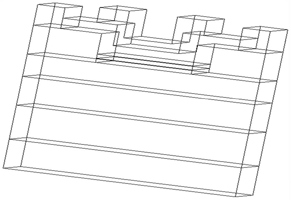
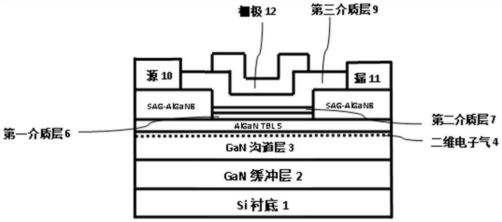
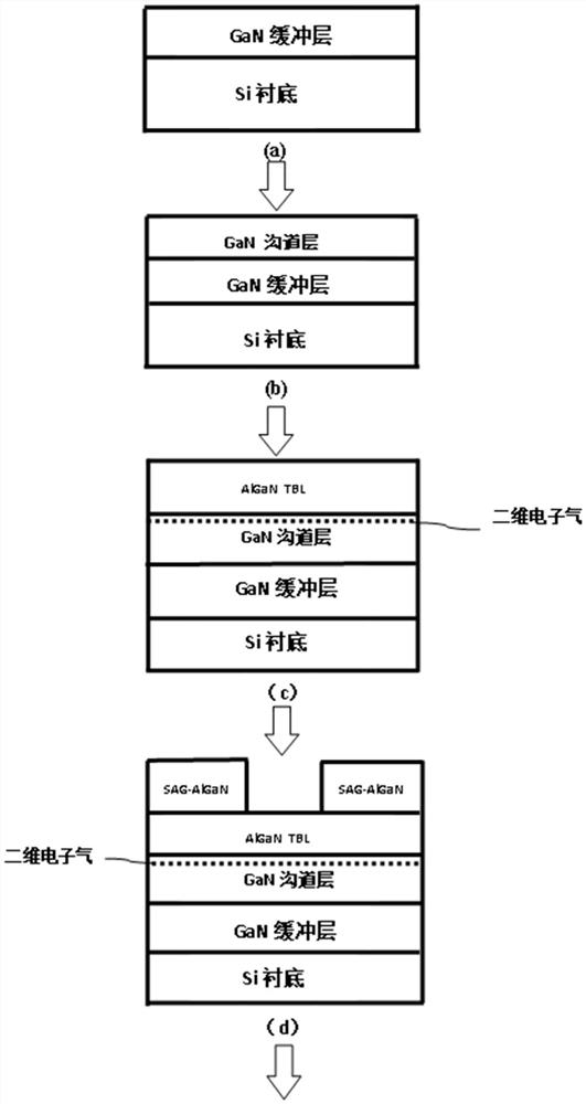
[0036] The present invention will be described in further detail below. like Figure 1-2 As shown, the enhanced GaN-based MIS-HEMT device of the present invention includes a GaN buffer layer 2, a GaN channel layer 3, an AlGaN thin barrier layer (AlGaNTBL) 5, and a concave AlGaN barrier layer stacked on a Si substrate 1 in sequence. (SAG-AlGaN) 8, the Al composition of the AlGaN thin barrier layer 5 is different from the concave AlGaN barrier layer 8, the GaN channel layer ...


PUM

PropertyMeasurementUnit
thicknessaaaaaaaaaa
thicknessaaaaaaaaaa
thicknessaaaaaaaaaa

Abstract

The invention relates to an enhanced GaN-based MIS-HEMT device and a preparation method thereof. In the MIS-HEMT device, a concave AlGaN barrier layer is arranged on the basis of a thin AlGaN barrierlayer, so that the channel mobility is improved, and the on resistance is improved. On the basis, an electron beam evaporation (EBE) method is adopted to grow a mask layer and is combined with an SAGmethod, compared with a PECVD mask used in a conventional process, the adoption of the EBE for growing the mask completely eliminates plasma damage in the mask technology, and damage-free crystal lattices are reserved for a thin AlGaN/GaN heterojunction. Meanwhile, the Al component of the AlGaN thin barrier layer is different from the Al component of the concave AlGaN barrier layer, and the threshold voltage and the channel electron mobility are further improved. In addition, a gate dielectric layer in the device is formed by stacking three oxide materials with different dielectric constants,the thickness of the dielectric layer is increased to ensure a certain threshold voltage, and the gate capacitance is increased by means of increasing the dielectric constant, so that the transconductance value is prevented from being too low.

Description

technical field [0001] The invention relates to the field of microelectronic technology, in particular to an enhanced GaN-based MIS-HEMT device and a preparation method thereof. Background technique [0002] GaN is a wide-bandgap semiconductor material. Because of its high saturation electron drift velocity, breakdown electric field strength, and high thermal conductivity, it can also form a heterojunction with AlGaN, and form a high-concentration, high-mobility secondary at the interface of the structure. Dimensional electron gas. Therefore, using GaN as a high-power, high-frequency device can make the on-resistance of the device small and the switching speed fast, and it has been widely used in the fields of wireless communication, radar and aerospace. [0003] In the application field of high-power transistors, GaN-based HEMT devices play a very important role. Due to the presence of strong polarized charges in the AlGaN / GaN heterojunction, it is difficult to fabricate ...

Claims


Application Information

Patent Timeline
Patent Type & Authority Applications(China)
IPC IPC(8): H01L29/778H01L29/06H01L29/205H01L29/423H01L29/51H01L21/335
CPCH01L29/778H01L29/0684H01L29/205H01L29/42316H01L29/513H01L29/66462
Inventor 孙慧卿夏凡夏晓宇谭秀洋马建铖张淼李渊
Owner SOUTH CHINA NORMAL UNIVERSITY
Why Eureka
Try Eureka