P-type organic semiconductor material, preparation method and display panel

An organic semiconductor and organic technology, applied in the field of P-type organic semiconductor materials, preparation methods and display panels, can solve the problems of high cost and difficult synthesis, and achieve low cost, improved hole mobility, and high degree of planarization Effect

Inactive Publication Date: 2020-09-04
WUHAN CHINA STAR OPTOELECTRONICS SEMICON DISPLAY TECH CO LTD
View PDF6 Cites 4 Cited by
  • Summary
  • Abstract
  • Description
  • Claims
  • Application Information

AI Technical Summary

Problems solved by technology

However, the synthesis of this P-type material is very difficult and costly.

Method used


Image

  • P-type organic semiconductor material, preparation method and display panel
  • P-type organic semiconductor material, preparation method and display panel
  • P-type organic semiconductor material, preparation method and display panel

Examples


preparation example Construction

[0048] The present application also provides a method for preparing a P-type organic semiconductor material, the preparation method comprising the following steps: making a first reactant containing a diketone undergo a cyclization reaction with a second reactant containing a diamine to generate the P type organic semiconductor materials;

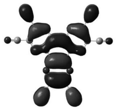
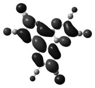
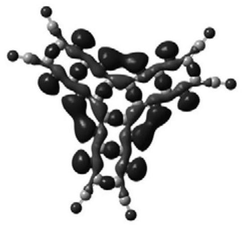
[0049] Wherein, the P-type organic semiconductor material has the following

[0050] The molecular structure represented, wherein, X is a carbon atom or a nitrogen atom; the R7, R8, R8, R10, R11, R12 are selected from the first substituent group;

[0051] When said R1 and said R2 are ring-opened, said R1 and said R2 are selected from said first substituent group,

[0052] When said R1 and said R2 form a ring, the structural formula after said R1 and said R2 form a ring is selected from A kind of, said group m1, m2, m3 and m4 are selected from the second substituent group;

[0053] When said R3 and said R4 are ring-opened, said R3 and ...

Embodiment 1

[0071] Cyclohexanone (0.98g, 10mmol), 5,6-diaminopiperidine-2,3-dicyano (12.01g, 75mmol) and catalyst, specifically, the catalyst can be added to the reaction vessel using acetic acid (100mL) middle. Under the protection of argon, the reaction was heated for 2h. The obtained mixture is hot filtered, washed and dried, and the solvent for washing may be hot acetic acid. The target product 1 was obtained by separation and purification. The method of separation and purification can be to use 200-300 mesh silica gel column chromatography on the crude product, the eluent is dichloromethane (DCM) decolorization, rotary evaporation, and vacuum drying to obtain a dark brown solid, and then sublimate to obtain a light yellow solid , which is the target product 1

[0072] The mass of the obtained target product 1 was 2.68 g, and the yield was 81%.

[0073] HRMS[M+H]+calcd.for C24N18:540.0553;found:540.0534.

[0074] The chemical equation for the reaction is:

[0075]

Embodiment 2

[0077] (0.98 g, 10 mmol), 4,5-diamino-3,6-difluorophthalonitrile (14.55 g, 75 mmol) and acetic acid (100 mL) were added to the reaction vessel. Under the protection of argon, the reaction was heated for 2h. The obtained mixture is hot filtered, washed and dried, and the solvent for washing may be hot acetic acid. The target product 2 was obtained by separation and purification. The method of separation and purification can be to use 200-300 mesh silica gel column chromatography on the crude product, the eluent is dichloromethane (DCM) decolorization, rotary evaporation, and vacuum drying to obtain a dark brown solid, and then sublimate to obtain a light yellow solid , which is the target product 2 The mass of the obtained target product 2 was 2.63 g, and the yield was 82%.

[0078] HRMS[M+H]+calcd.for C30F6N12:642.0273;found:642.0277.

[0079] The chemical equation for the reaction is:

[0080]


PUM

PropertyMeasurementUnit
thicknessaaaaaaaaaa
thicknessaaaaaaaaaa
thicknessaaaaaaaaaa

Abstract

The invention provides a P-type organic semiconductor material, a preparation method and a display panel. According to the P-type organic semiconductor material, substituent groups are used for replacing hydrogen on a ring in a molecular structure, and the LUMO energy level of the obtained P-type organic semiconductor material is reduced. When the P-type organic semiconductor material is used as ahole injection layer and a hole transport layer of a light emitting device, the ability of the hole transport layer to form holes is enhanced, the injection of the holes from an anode to the hole transport layer is improved, and the hole mobility is improved accordingly, so that the driving voltage of the light emitting device can be reduced. On the other hand, the molecular structure planarization degree of the P-type organic semiconductor material is high, the hole mobility can be further improved, and hole injection and transmission are facilitated. The preparation method of the P-type organic semiconductor material provided by the invention is simple in synthesis steps and low in cost.

Description

technical field [0001] The present application relates to the field of organic light emitting diodes, in particular to a P-type organic semiconductor material, a preparation method and a display panel. Background technique [0002] A known organic light emitting diode device includes an anode, a hole injection layer, a hole transport layer, a light emitting layer, an electron injection layer, an electron transport layer and a cathode. When the organic light-emitting diode device is energized, electron carriers are generated from the cathode and injected into the electron injection layer, and then reach the light-emitting layer through the electron transport layer; while hole carriers are generated from the anode and injected into the hole injection layer, and pass through the hole transport layer. The layer reaches the light-emitting layer; electron carriers and hole carriers recombine in the light-emitting layer or the interface between the light-emitting layer and the tran...

Claims


Application Information

Patent Timeline
Patent Type & Authority Applications(China)
IPC IPC(8): C07D487/22C07D487/14C07D487/04H01L51/50H01L51/54
CPCC07D487/22C07D487/14C07D487/04H10K85/6572H10K50/17H10K2102/351
Inventor 王彦杰
Owner WUHAN CHINA STAR OPTOELECTRONICS SEMICON DISPLAY TECH CO LTD
Why Eureka
Try Eureka