Chip connection method for rapidly generating high-strength and high-melting-point joint at low temperature

A connection method and high-strength technology, applied in the manufacture of electrical components, electrical solid-state devices, semiconductor/solid-state devices, etc., to achieve the effects of high service temperature, high reliability, and reduced production costs

Inactive Publication Date: 2020-09-04
HARBIN INSTITUTE OF TECHNOLOGY SHENZHEN (INSTITUTE OF SCIENCE AND TECHNOLOGY INNOVATION HARBIN INSTITUTE OF TECHNOLOGY SHENZHEN)
View PDF7 Cites 5 Cited by
  • Summary
  • Abstract
  • Description
  • Claims
  • Application Information

AI Technical Summary

Problems solved by technology

[0004] At present, the introduction of high-energy ultrasound to sinter nano-solder at low temperature to achieve a fast and efficient connection process has not been reported, especially the use of metal nanoparticles as the intermediate layer solder to achieve ultra-low temperature connection and high-temperature service under the action of high-energy ultrasound. , the process has the advantages of high efficiency, high strength, high reliability and high temperature stability

Method used


Image

  • Chip connection method for rapidly generating high-strength and high-melting-point joint at low temperature
  • Chip connection method for rapidly generating high-strength and high-melting-point joint at low temperature
  • Chip connection method for rapidly generating high-strength and high-melting-point joint at low temperature

Examples


Embodiment 1

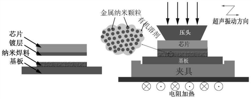
[0036] refer to figure 1 As shown, a chip connection method for quickly producing high-strength and high-melting point joints at low temperature, the connection materials mainly include: chip-1 with Ni / Ag plating layer, nano-silver-coated copper solder intermediate layer-2 and a copper substrate with a size of 10×10mm -3, is characterized in that comprising the following steps:

[0037] (1) Surface treatment of the material to be connected: According to the pre-set ion cleaning process: RF power 200W, RF time 150s, keep the cavity pressure at -100Pa, then chip-1 with Ni / Ag plating and copper Substrate-3 is cleaned with ions on the metal surface to remove the oxide layer and surface organic matter, and then ultrasonically cleaned for 30s to expose the clean metal surface for later use;

[0038] (2) After setting the height and basic level of the scraping head in advance, use the gravure printing process to evenly coat the configured nano silver-clad copper solder paste on the ...

Embodiment 2

[0045] refer to figure 1 As shown, a chip connection method for quickly producing high-strength and high-melting point joints at low temperature, the connection materials mainly include: chip-1 with Ni / Ag plating layer, nano-silver-coated copper solder intermediate layer-2 and a copper substrate with a size of 10×10mm -3, is characterized in that comprising the following steps:

[0046] (1) Surface treatment of the material to be connected: According to the pre-set ion cleaning process: RF power 200W, RF time 150s, keep the cavity pressure at -100Pa, then chip-1 with Ni / Ag plating and copper Substrate-3 is cleaned with ions on the metal surface to remove the oxide layer and surface organic matter, and then ultrasonically cleaned for 30s to expose the clean metal surface for later use;

[0047] (2) After setting the height and basic level of the scraping head in advance, use the gravure printing process to evenly coat the configured nano silver-clad copper solder paste on the ...

Embodiment 3

[0053] refer to figure 1 As shown, a chip connection method for quickly producing high-strength and high-melting point joints at low temperature, the connection materials mainly include: chip-1 with Ni / Ag plating layer, nano-silver-coated copper solder intermediate layer-2 and a copper substrate with a size of 10×10mm -3, is characterized in that comprising the following steps:

[0054] (1) Surface treatment of the material to be connected: According to the pre-set ion cleaning process: RF power 200W, RF time 150s, keep the cavity pressure at -100Pa, then chip-1 with Ni / Ag plating and copper Substrate-3 is cleaned with ions on the metal surface to remove the oxide layer and surface organic matter, and then ultrasonically cleaned for 30s to expose the clean metal surface for later use;

[0055] (2) After setting the height and basic level of the scraping head in advance, use the gravure printing process to evenly coat the configured nano silver-clad copper solder paste on the ...


PUM

PropertyMeasurementUnit
viscosityaaaaaaaaaa
thicknessaaaaaaaaaa
shear strengthaaaaaaaaaa

Abstract

The invention discloses a chip connection method for rapidly generating a high-strength and high-melting-point joint at a low temperature. A self-designed resistance heating and power ultrasonic combined ultrasonic auxiliary hot-pressing device is adopted to realize low-temperature chip connection without damage on the chip. In the chip connection process, severe friction is generated between metal nanoparticles and between the particles and a substrate through a physical vibration effect of ultrasonic waves, the temperature of a solder layer is rapidly increased, atom diffusion is accelerated, and finally connection between the chip and the substrate is achieved at a lower temperature within an extremely short time. The joint obtained through the method has higher shear strength (70-90 MPa), high thermal conductivity (60-80 W / m.K) and wide service temperature, is an effective solution for third-generation semiconductor chip connection, and meanwhile meets the special application occasions of long-time high service temperature, high strength and high reliability.

Description

Technical field: [0001] The invention belongs to a new type of chip connection technology, in particular to a chip connection method for rapidly generating high-strength and high-melting point joints at low temperature, which can be applied to the surface mount technology of various components. Background technique: [0002] In the field of microelectronic packaging, the development trend of semiconductor chips is bound to advance in the direction of miniaturization, high integration, and high power density, and higher and more stringent requirements are put forward for devices, such as: high temperature, high current and harsh environment This poses a great challenge to traditional chip interconnection. In addition, with the rapid development of the third-generation semiconductor materials with unique properties such as wide bandgap, high thermal conductivity, high breakdown voltage, and good chemical stability represented by SiC and GaN, especially in aerospace, power A l...

Claims


Application Information

Patent Timeline
Patent Type & Authority Applications(China)
IPC IPC(8): H01L21/48H01L21/60
CPCH01L21/4871H01L24/27H01L2224/27013H01L2224/2711H01L2224/2781H01L2224/27848
Inventor 计红军张文武修子进马秋晨曹依琛潘浩张琳李明雨
Owner HARBIN INSTITUTE OF TECHNOLOGY SHENZHEN (INSTITUTE OF SCIENCE AND TECHNOLOGY INNOVATION HARBIN INSTITUTE OF TECHNOLOGY SHENZHEN)
Why Eureka
Try Eureka