Silicon substrate nitride multi-quantum well homogeneously integrated electro-optical modulator and preparation method thereof

An electro-optic modulator and multi-quantum well technology, which is applied in optics, instruments, circuits, etc., can solve the problems of low electro-optic modulation efficiency and leakage, and achieve the effects of improving high optical field constraints, improving efficiency, reducing optical loss and light leakage

Inactive Publication Date: 2020-09-04
NANJING UNIV OF POSTS & TELECOMM
View PDF0 Cites 3 Cited by
  • Summary
  • Abstract
  • Description
  • Claims
  • Application Information

AI Technical Summary

Problems solved by technology

In this case, when designing an electro-optic modulator, only a part of the outgoing light generated in the micro-LED designed based on the multi-quantum well structure can be coupled into the waveguide-type electro-optic modulator module for electro-optic modulation, and the remaining visible light signal will leak into the The thicker nitride epitaxial layer and silicon substrate under the multi-quantum well structure make the electro-optic modulation efficiency lower

Method used


Image

  • Silicon substrate nitride multi-quantum well homogeneously integrated electro-optical modulator and preparation method thereof
  • Silicon substrate nitride multi-quantum well homogeneously integrated electro-optical modulator and preparation method thereof
  • Silicon substrate nitride multi-quantum well homogeneously integrated electro-optical modulator and preparation method thereof

Examples


Embodiment Construction

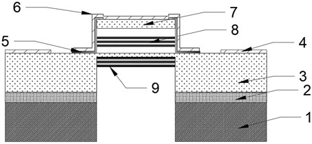
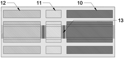
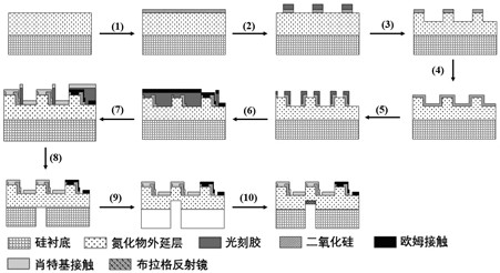
[0031] see figure 1 with figure 2 , the present embodiment provides an electro-optic modulator for the homogeneous integration of silicon substrate nitride multi-quantum wells, using a nitride wafer with a multi-quantum well structure as a carrier, including a silicon substrate layer (1), including a multi-quantum well ( 8) the top nitride epitaxial layer and the single-wavelength light source (10), electro-optic modulator (11) and photodetection module (12) arranged in the top nitride epitaxial layer; the two ends of the electro-optic modulator (11) pass through The planar waveguide (13) is connected to the single-wavelength light source (10) and the photodetection module (12), the substrate layer (1) below the electro-optic modulator (11) is hollowed out, and the top nitride epitaxial layer is thinned to form a suspended nitride film; a Bragg reflector (9) is arranged under the suspended nitride film. Using III-V material ICP etching inductively coupled plasma etching tec...


PUM

PropertyMeasurementUnit
wavelengthaaaaaaaaaa

Abstract

The invention discloses a silicon substrate nitride multi-quantum well homogeneously integrated electro-optical modulator and a preparation method thereof. A silicon substrate nitride wafer with a multi-quantum well structure as a carrier is realized, the silicon substrate nitride wafer with the multi-quantum well structure comprises a silicon substrate layer and a nitride epitaxial layer which islocated on the silicon substrate layer and comprises the multi-quantum well structure, and a waveguide type electro-optical modulation module which serves as a single-wavelength light source and is provided with a Bragg reflector and a photoelectric detector are arranged on the nitride epitaxial layer. The light source, the electro-optical modulation module and the photoelectric detector are integrated on a suspended film structure, visible light transmission loss and transmission leakage in the homogeneously integrated electro-optical modulator are low, and optical signals can be controlledand modulated with high degree-of-freedom and high response speed. The electro-optical modulator can applied to an optical communication network to improve performance indexes of a visible light communication technology in the aspects such as information transmission rate, information processing speed and terminal device integration degree.

Description

technical field [0001] The invention belongs to the technical field of information materials and devices, and in particular relates to an electro-optic modulator and a preparation method for the homogeneous integration of silicon substrate nitride multi-quantum wells. Background technique [0002] Visible light communication is an optical wireless communication technology that utilizes the high-speed response characteristics of LED output optical power and driving current, uses visible light as an information carrier, and realizes high-speed data communication functions. Compared with traditional communication methods, visible light communication technology has high transmission frequency, extremely low energy consumption, high security and good confidentiality, and can quickly build an anti-jamming and anti-interception security information space. As one of the key devices for controlling and modulating the intensity of visible light signals in visible light communication, ...

Claims


Application Information

Patent Timeline
Patent Type & Authority Applications(China)
IPC IPC(8): H01L31/173H01L31/18G02F1/017G02F1/03
CPCG02F1/017G02F1/0305H01L31/173H01L31/1852H01L31/1856Y02P70/50
Inventor 李欣吴悦蒋成伟沙源清王永进
Owner NANJING UNIV OF POSTS & TELECOMM
Why Eureka
Try Eureka