CMOS protective layer structure and manufacturing method thereof

A manufacturing method and protective layer technology, applied in radiation control devices, electrical components, electrical solid devices, etc., can solve problems such as metal pollution and affecting device performance

Pending Publication Date: 2020-10-16
SHANGHAI HUALI INTEGRATED CIRCUTE MFG CO LTD
View PDF4 Cites 0 Cited by
  • Summary
  • Abstract
  • Description
  • Claims
  • Application Information

AI Technical Summary

Problems solved by technology

[0009] In the prior art, after depositing the protective layer, the WAT Test was performed, and the bump defect

Method used


Image

  • CMOS protective layer structure and manufacturing method thereof
  • CMOS protective layer structure and manufacturing method thereof

Examples


Example

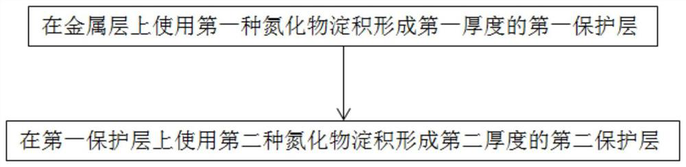
[0034] The first embodiment, such as figure 1 Said, the CMOS protection layer structure provided by the present invention, it is formed on the metal layer of CMOS, comprises:

[0035] a first protection layer deposited on the metal layer and having a thickness of a first thickness;

[0036] a second protection layer deposited on the first protection layer and having a thickness of a second thickness;

[0037] Wherein, the first protection layer and the second protection layer are nitride layers formed by depositing different materials, the second thickness is greater than the first thickness, and the temperature required for depositing the first protection layer is lower than the temperature required for depositing the second protection layer .

[0038] The first embodiment of the present invention can reduce the formation of bump defects well by reducing the metal precipitation degree. Therefore, depositing the first protective layer on the metal layer can effectively red...

Example

[0039] In the second embodiment, the CMOS protection layer structure provided by the present invention is formed on the metal layer of CMOS, including:

[0040] A carbon silicon compound layer is deposited and formed on the metal copper layer, and its thickness ranges from 100 angstroms to 150 angstroms;

[0041] A silicon nitride layer is deposited on the silicon nitride carbon compound layer, and its thickness ranges from 2000 angstroms to 3000 angstroms.

Example

[0042] In the third embodiment, the CMOS protection layer structure provided by the present invention is formed on the metal layer of CMOS, including:

[0043] A carbon silicon compound layer is deposited and formed on the metal copper layer with a thickness of 130 angstroms;

[0044] A silicon nitride layer is deposited on the silicon nitride layer to a thickness in the range of 2370 Angstroms.


PUM

PropertyMeasurementUnit
Thicknessaaaaaaaaaa
Thicknessaaaaaaaaaa
Thicknessaaaaaaaaaa

Abstract

The invention discloses a CMOS protective layer structure, which is formed on a metal layer of a CMOS and comprises a first protective layer and a second protective layer, wherein the first protectivelayer is formed on the metal layer in a deposition mode and has a first thickness; the second protective layer is formed on the first protective layer in a deposition mode, and the thickness of the second protective layer is a second thickness; the first protective layer and the second protective layer are nitride layers formed by deposition of different materials, the second thickness is largerthan the first thickness, and the temperature required for deposition of the first protective layer is lower than the temperature required for deposition of the second protective layer. After the method is used for the CMOS metal process, the defect of bumps formed by metal precipitation can be avoided, the uniformity and the stability of the CMOS can be improved, and the yield can be further improved.

Description

technical field [0001] The invention relates to the field of semiconductor manufacturing, in particular to a protective layer structure for CMOS (Complementary Metal Oxide Semiconductor). The invention also relates to a manufacturing method for a CMOS (Complementary Metal Oxide Semiconductor) protective layer structure. Background technique [0002] An existing CMOS image sensor (CMOS Image Sensor, CIS) includes a pixel unit circuit and a CMOS circuit. Compared with CCD image sensors, CMOS image sensors have better integration because they adopt CMOS standard manufacturing process, and can be integrated with other digital-analog operations and control circuits on the same chip, which is more adaptable to future development. [0003] The manufacturing method of the existing CMOS image sensor mainly includes the following steps: [0004] Step 1. Simultaneously form gate dielectric layers, such as gate oxide layers and polysilicon gates, of each MOS transistor of the pixel un...

Claims


Application Information

Patent Timeline
IPC IPC(8): H01L27/146
CPCH01L27/1462H01L27/14685H01L27/14689
Inventor 陈则同林聪徐莹
Owner SHANGHAI HUALI INTEGRATED CIRCUTE MFG CO LTD
Why Eureka
Try Eureka