Resonant tunneling diode and manufacturing method thereof
A technology of resonant tunneling and fabrication methods, which is applied in the fields of diodes, semiconductor/solid-state device manufacturing, electrical components, etc., can solve the problems of large differences in activity, performance defects of resonant tunneling diodes, insufficient power of resonant tunneling diodes, etc. Lattice mismatch, the effect of increasing power
- Summary
- Abstract
- Description
- Claims
- Application Information
AI Technical Summary
Problems solved by technology
Method used
Image
Examples
Embodiment 1
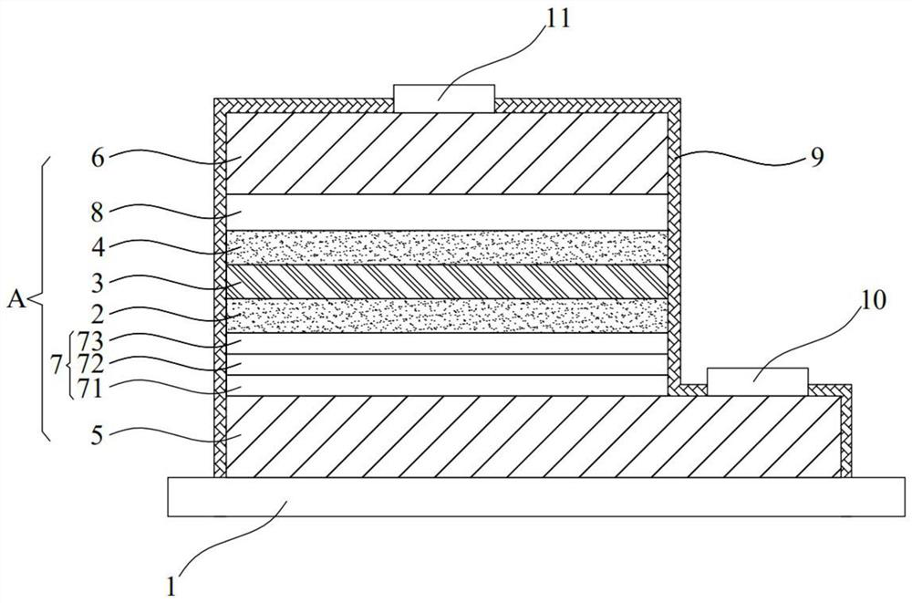
[0027] This embodiment provides a resonant tunneling diode, such as figure 1 As shown, the resonant tunneling diode includes a substrate 1 and an epitaxial portion A formed on the substrate 1 . The epitaxial part A includes a first barrier layer 2 , a potential well layer 3 and a second barrier layer 4 sequentially stacked on the substrate 1 . Wherein, the potential well layer 3 of this embodiment is made of GaN material, and the first barrier layer 2 and the second barrier layer 4 are both made of AlN material. In this embodiment, in order to overcome the problem of large lattice mismatch between GaN material and AlN material, when growing the potential well layer 3, the first barrier layer 2 and the second barrier layer 4, molecular beam epitaxy process.
[0028] Specifically, the epitaxial portion A further includes a first electrode 10 and a second electrode 11 for conducting with external electronic devices. In order to provide a good environment for current transmissi...
Embodiment 2
[0033] This embodiment provides a specific manufacturing method of the resonant tunneling diode of the first embodiment. The manufacturing method includes: sequentially stacking and forming a first barrier layer 2, a potential well layer 3 and a second barrier layer 4 on a substrate 1 by using a molecular beam epitaxy process; wherein, the first barrier layer 2 and The growth material of the second barrier layer 4 is AlN material, and the growth material of the potential well layer 3 is GaN material.
[0034] Specifically, such as Figure 2a to Figure 2g As shown, the preparation method specifically includes:
[0035] A substrate 1 is provided, and the substrate 1 is preferably a GaN substrate.
[0036] A first ohmic contact layer 5 is formed on the substrate 1 . Specifically, the first ohmic contact layer 5 is grown on the substrate 1 by molecular beam epitaxy. Wherein, the growth material is GaN material heavily doped with Si, and the Si doping concentration of the GaN m...
PUM
| Property | Measurement | Unit |
|---|---|---|
| Thickness | aaaaa | aaaaa |
| Growth thickness | aaaaa | aaaaa |
Abstract
Description
Claims
Application Information
 - R&D Engineer
- R&D Manager
- IP Professional
- Industry Leading Data Capabilities
- Powerful AI technology
- Patent DNA Extraction
Browse by: Latest US Patents, China's latest patents, Technical Efficacy Thesaurus, Application Domain, Technology Topic, Popular Technical Reports.
© 2024 PatSnap. All rights reserved.Legal|Privacy policy|Modern Slavery Act Transparency Statement|Sitemap|About US| Contact US: help@patsnap.com


