Hydrophobic material protected by microstructure as well as preparation method and application thereof
A hydrophobic material, microstructure technology, applied in microstructure technology, microstructure device, manufacturing microstructure device, etc., can solve the problem of easy damage, short service life, poor light transmittance, wear resistance, etc. question
- Summary
- Abstract
- Description
- Claims
- Application Information
AI Technical Summary
Problems solved by technology
Method used
Image
Examples
preparation example Construction
[0056] Preparation method of microstructure
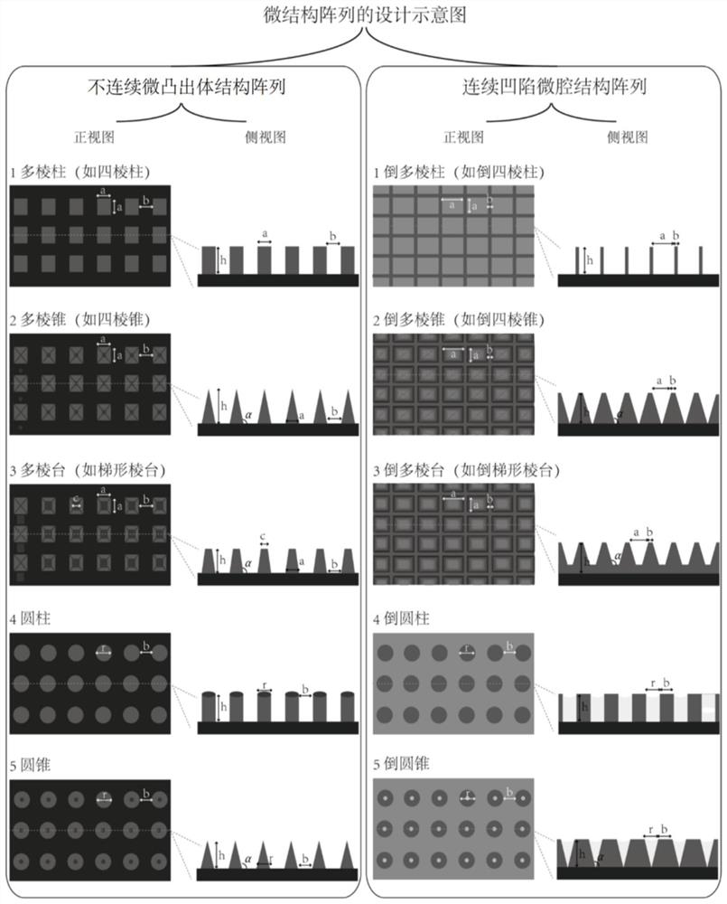
[0057] The method of preparing the microstructure on the substrate is not limited, and can be selected according to the nature of the substrate itself. For example, the microstructure can be directly prepared by microfabrication techniques such as photolithography, micromilling, or the mold can be made first, and then the microstructure can be indirectly prepared by the method of transferring the pattern to the substrate by cold / hot pressing technology.
[0058] Method of filling hydrophobic filler
[0059] According to the specific morphology of the microstructure, the hydrophobic filler can be filled in the gaps between the microstructure units by vapor deposition, spin coating / spraying, evaporation, or magnetron sputtering. The hydrophobic filler can fill all the voids between the microstructure units, or can only fill a part of it. For example, the hydrophobic filler forms a thin layer to cover the surface of the microstructure unit ...
Embodiment 1
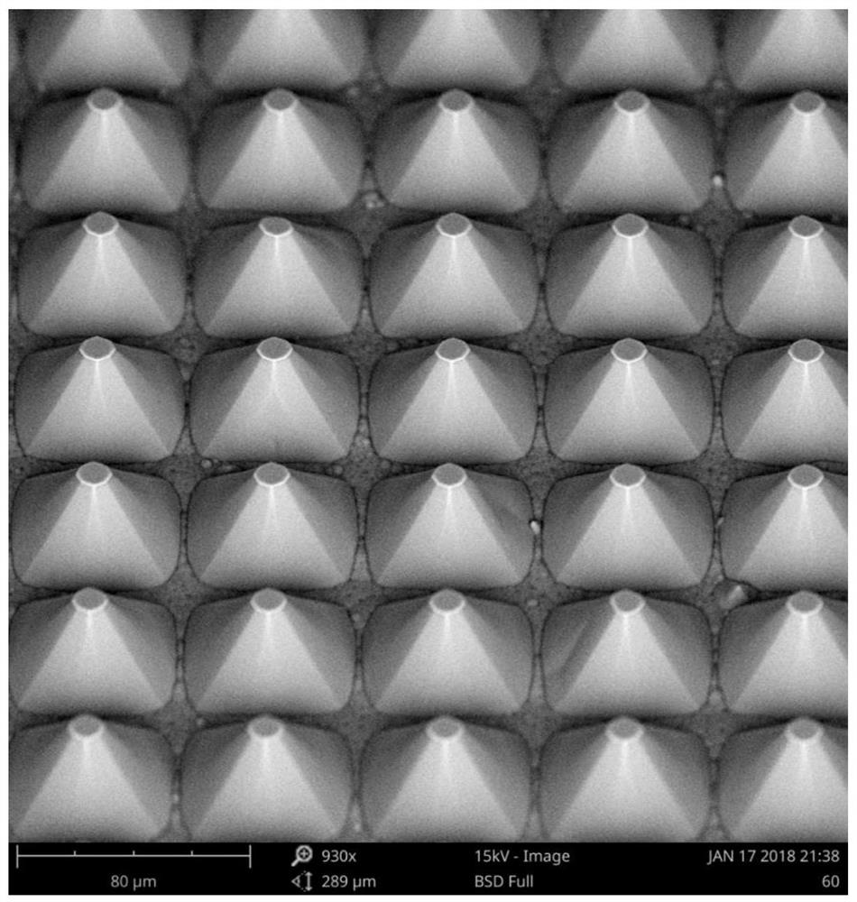
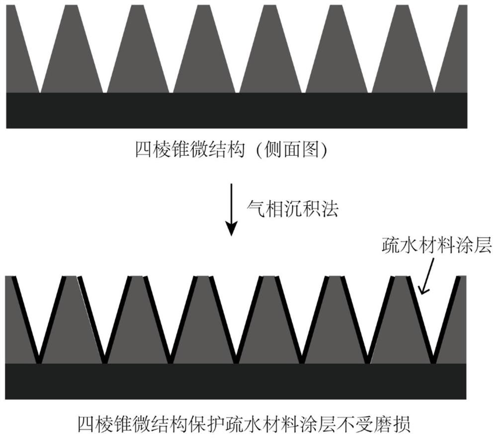
[0064] The hydrophobic material prepared in this embodiment includes an array composed of discontinuous quadrangular pyramid microstructure units prepared on a silicon substrate (such as figure 2 (Shown), there is a polymer hydrophobic filler between the microstructure units. The sidewall angle of the quadrangular pyramid is 125°, the side length of the quadrangular pyramid is 60μm, the height is 40μm, and the interval between adjacent quadrangular pyramids is 3.5μm; the microstructure is prepared by photolithography and wet etching on the silicon substrate, and the Hydrophobic fillers are deposited in the microstructure frame for protection by vapor deposition, such as image 3 Shown.
[0065] The preparation of the silicon substrate quadrangular pyramid microstructure-photolithography and wet etching, the process steps are: firstly treat the silicon wafer with plasma for 30 minutes, and then bake the wafer at 260°C for 30 minutes. After the treated silicon wafer was uniformly ...
Embodiment 2
[0069] The hydrophobic material prepared in this embodiment includes a silicon substrate as the substrate to be filled. On the silicon wafer substrate, a quadrangular pyramid microstructure is prepared by photolithography and wet etching methods (the method is the same as in Example 1), and the hydrophobic filler is filled by spin coating. Inside the microstructure.
[0070] Filling of hydrophobic material-spin coating method, the specific steps are: the microstructured silicon wafer is subjected to acetone, alcohol, and deionized water ultrasonic treatment for 5 minutes. Then it was placed on a spin coater, and fluorinated oil WP140 was spin-coated at a speed of 3000 rpm for 20 seconds. Finally, put the filled silicon wafers in an oven at 60°C for drying.
[0071] The surface of the microstructured hydrophobic material prepared in this example was subjected to 20 scratch experiments with a blade. The results show that the surface of the hydrophobic material prepared in this exam...
PUM
| Property | Measurement | Unit |
|---|---|---|
| depth | aaaaa | aaaaa |
| height | aaaaa | aaaaa |
| depth | aaaaa | aaaaa |
Abstract
Description
Claims
Application Information


