A self-aligned gan Schottky diode and its manufacturing method
A technology for Schottky diodes and manufacturing methods, which is applied in the fields of diodes, semiconductor/solid-state device manufacturing, semiconductor devices, etc., can solve the problems of low plane process compatibility, current crowding, and complicated manufacturing processes, and achieves strong manufacturability, high The effect of shortened pitch and low process complexity
- Summary
- Abstract
- Description
- Claims
- Application Information
AI Technical Summary
Problems solved by technology
Method used
Image
Examples
Embodiment 1
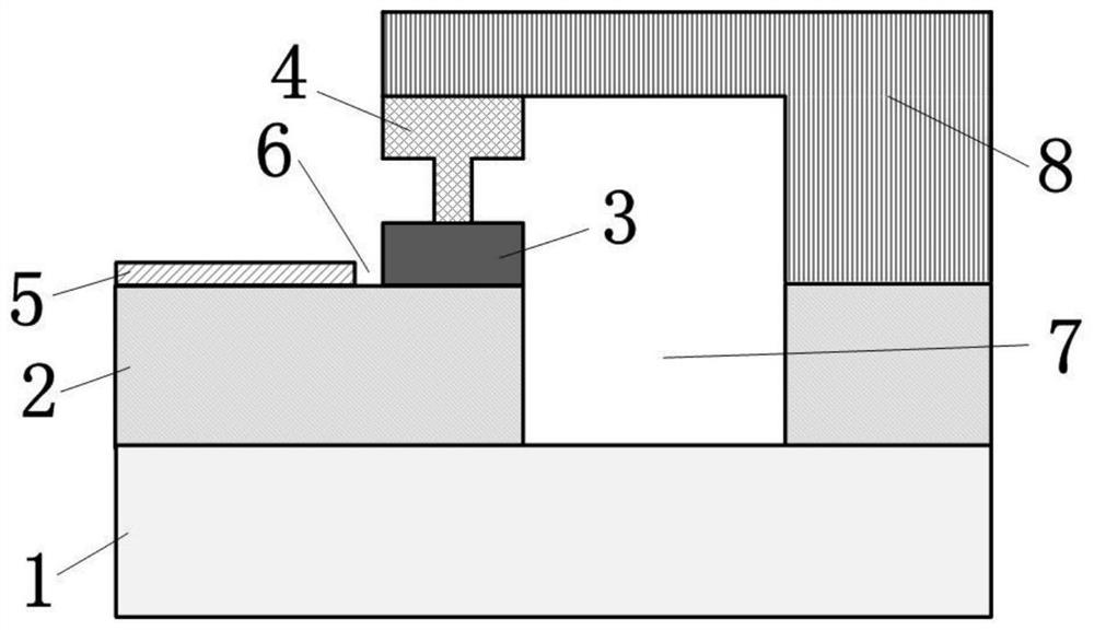
[0044] Example 1: Preparation The SiC substrate 1 is used, the width of the spacer 6 is 150 nm, the metal of the T-type anode 4 is Ni / Pt / Au, and the doping concentration of the n-GaN layer 3 is 2E17 / cm 3 , the doping concentration of n+GaN layer 2 is 5E19 / cm 3 Specifications of a self-aligned GaN Schottky diode whose fabrication process is:
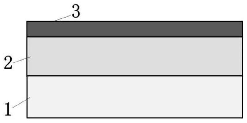
[0045] 1) On the SiC substrate 1, use the metal organic chemical vapor deposition technology MOCVD to grow a 1 μm thick n+GaN layer 2 at 950 ° C, the doping source is Si, and the doping concentration is 5E19 / cm 3 , and then grow a 1 μm thick n-GaN layer 3, the doping source is Si, and the doping concentration is 2E17 / cm 3 .
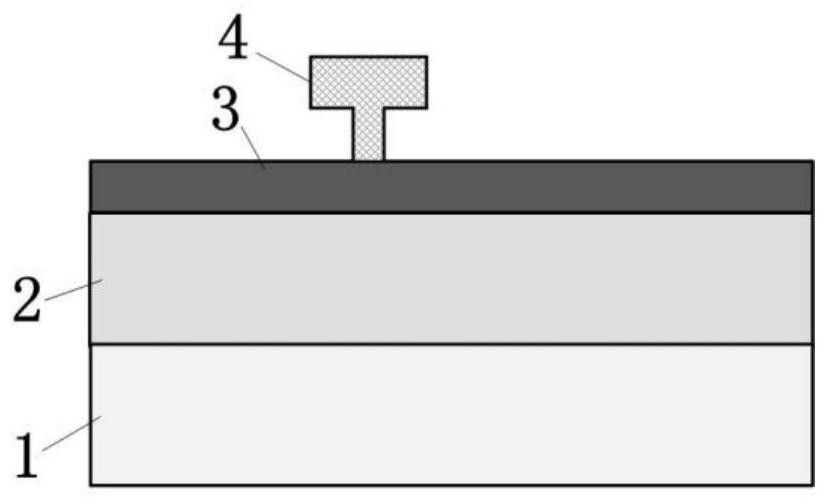
[0046] 2) The anode pattern is photoetched on the top of the n-GaN layer 3, and then the anode metal is evaporated to form a T-type anode 4; It is 30nm, 50nm and 600nm; the process conditions of electron beam evaporation are: vacuum degree≤2.0×10 -6 Torr, the deposition rate is less than
[0047] 3) Using the ...
Embodiment 2
[0053] Example 2: Preparation The Si substrate 1 is used, the width of the spacer 6 is 20 nm, the metal of the T-type anode 4 is W / Ti / Au, and the doping concentration of the n-GaN layer 3 is 5E17 / cm 3 , the doping concentration of n+GaN layer 2 is 4E20 / cm 3 Specifications of a self-aligned GaN Schottky diode whose fabrication process is:
[0054] 1) On the SiC substrate 1, use the metal organic chemical vapor deposition technology MOCVD to grow a 2 μm thick n+GaN layer 2 at 950 ° C, the doping source is Ge, and the doping concentration is 4E20 / cm 3 , and then grow a 300nm thick n-GaN layer 3, the doping source is Ge, and the doping concentration is 5E17 / cm 3 .
[0055] 2) The anode pattern is photoetched on the top of the n-GaN layer 3, and then the anode metal is sputtered to form a T-type anode 4; It is 20nm, 20nm and 700nm; the process conditions of magnetron sputtering are: vacuum degree≤3×10 -6 Torr, the deposition rate is less than
[0056] 3) Step 3) of Example 2...
PUM
| Property | Measurement | Unit |
|---|---|---|
| width | aaaaa | aaaaa |
| thickness | aaaaa | aaaaa |
| thickness | aaaaa | aaaaa |
Abstract
Description
Claims
Application Information


