

Preparation method of passivation contact solar cell
A solar cell, passivation reduction technology, applied in the direction of circuits, photovoltaic power generation, electrical components, etc., can solve the problems of increasing process steps, reducing solar cell production capacity, and reducing solar cell quality
- Summary
- Abstract
- Description
- Claims
- Application Information
AI Technical Summary
Problems solved by technology
Method used
Image

Examples
preparation example Construction
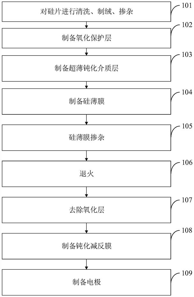
[0038] Such as figure 1 As shown, the embodiment of the present invention provides a method for preparing a passivated contact solar cell, comprising the following steps:
[0039] Step 101, cleaning, texturing and doping the silicon wafer.
[0040] Step 102 , preparing an oxidation protection layer 33 .
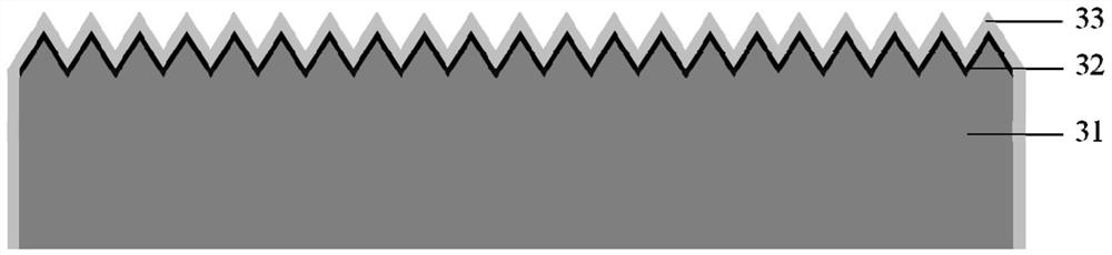
[0041] In the embodiment of the present invention, the doped surface is protected by low-temperature furnace tube oxidation process, or nitric acid oxidation process, or ozone oxidation process, or atomic layer deposition (ALD) growth, or low-pressure chemical vapor deposition (LPCVD) in-situ growth oxidation protection. layer. The oxidation protection layer includes: a single-layer film or a laminated film of several kinds of silicon oxide, titanium oxide and silicon oxynitride. Compared with the existing technology, the oxidation protection layer not only covers the doped surface, but also covers the side of the silicon wafer, such as figure 2 shown.
[0042] It shoul...
Embodiment 1
[0062] This example illustrates a preparation process for a high-performance passivated contact solar cell, and the specific steps are as follows:
[0063] 1. Cleaning, texturing, and doping: select an N-type single crystal silicon substrate with a resistivity of 0-30Ω·cm and a thickness of 50-300μm. After cleaning and texturing one side of the silicon wafer 31, the silicon The sheet is doped to form a doped layer 32, and the boron (B) doping concentration range is 1.0E19atoms / cm 3 -2.0E21 atoms / cm 3 , and then use the temperature of 1000°C to advance and diffuse the doped B;
[0064] 2. Preparing and depositing an oxidation protection layer 33: using low-pressure chemical deposition (LPCVD) equipment, growing a 50nm oxidation protection layer 33 in situ on the doped surface of the silicon wafer, which can be an oxide layer (SiO 2 ), after completing this step, if figure 2 shown.
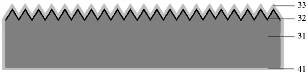
[0065] 3. Preparation of low-pressure chemical deposition (LPCVD) ultra-thin passivation di...
Embodiment 2
[0073] This example illustrates a preparation process for a high-performance passivated contact solar cell, and the specific steps are as follows:
[0074] 1. Cleaning, texturing, and doping: select an N-type single crystal silicon substrate with a resistivity of 0-30Ω·cm and a thickness of 50-300μm. After cleaning and texturing one side of the silicon wafer 31, the silicon The sheet is doped to form a doped layer 32, and the boron (B) doping concentration range is 1.0E19atoms / cm 3 -2.0E21 atoms / cm 3 , and then use the temperature of 1000°C to advance and diffuse the doping B.
[0075] 2. Preparing and depositing an oxidation protection layer 33: using low-pressure chemical deposition (LPCVD) equipment, growing a 100nm oxidation protection layer 33 in situ on the doped surface of the silicon wafer, which can be an oxide layer (SiO 2 ), after completing this step, if figure 2 shown.
[0076] 3. Preparation of low-pressure chemical deposition (LPCVD) ultra-thin passivation ...
PUM
| Property | Measurement | Unit |
|---|---|---|
| Thickness range | aaaaa | aaaaa |
| Resistivity | aaaaa | aaaaa |
| Thickness | aaaaa | aaaaa |
Abstract
Description
Claims
Application Information