Organic compound, and electronic element and electronic device using same

An organic compound, fusion technology, applied in the direction of silicon organic compounds, electrical components, organic chemistry, etc.

Active Publication Date: 2020-10-30
SHAANXI LIGHTE OPTOELECTRONICS MATERIAL CO LTD
View PDF2 Cites 10 Cited by
  • Summary
  • Abstract
  • Description
  • Claims
  • Application Information

AI Technical Summary

Problems solved by technology

[0004]In the existing organic electroluminescent devices, the main problems are life and efficiency. Efficiency and power efficiency also need to b

Method used


Image

  • Organic compound, and electronic element and electronic device using same
  • Organic compound, and electronic element and electronic device using same
  • Organic compound, and electronic element and electronic device using same

Examples


Embodiment approach

[0157] In one embodiment of the present application, the electronic component may be an organic electroluminescent device or a photoelectric conversion device.

[0158] In one embodiment of the present application, the electronic component may be an organic electroluminescence device.

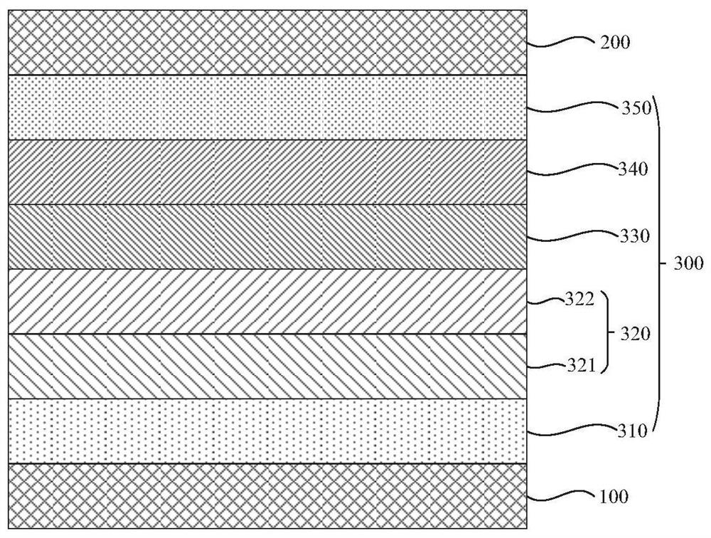
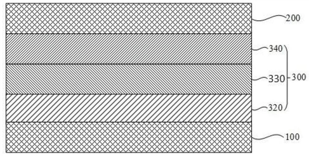
[0159] In one embodiment of the present application, the organic electroluminescence device may be a green device or a red device. Such as figure 1 As shown, the organic electroluminescent device may include an anode 100, a first hole transport layer 321, a second hole transport layer 322, an organic light-emitting layer 330 as an energy conversion layer, an electron transport layer 340, and a cathode 200 stacked in sequence. .

[0160] Optionally, the anode 100 includes the following anode material, which is preferably a material with a large work function (work function) that facilitates hole injection into the functional layer. Specific examples of anode materials include: metals such as ...

Synthetic example

[0182] 1. Preparation of intermediate a-1

[0183]

[0184] 2-Bromo-4-chloro-1-iodobenzene (50.0g, 157.5mmol), dibenzofuran-3-boronic acid (30.4g, 157.5mmol), tetrakis(triphenylphosphine) palladium (3.6g, 3.1 mmol), potassium carbonate (54.3g, 393.8mmol), tetrabutylammonium bromide (10.1g, 31.5mmol) were added in the flask, and a mixed solvent of toluene (440mL), ethanol (200mL) and water (100mL) was added, Under nitrogen protection, raise the temperature to 80°C, keep the temperature and stir for 24 hours, cool to room temperature, stop stirring, wash the reaction solution with water, separate the organic phase, dry with anhydrous magnesium sulfate, and remove the solvent under reduced pressure to obtain the crude product; use dichloromethane / n-heptane was purified by silica gel column chromatography as the mobile phase crude product to obtain intermediate a-1 (33.8 g, 60%) as a white solid product.

[0185] Substitute reactant A in Table 1 for 2-bromo-4-chloro-1-iodoben...

Embodiment 1

[0257] Embodiment 1: green organic electroluminescent device

[0258] Use the following methods to fabricate green organic electroluminescent devices:

[0259] The anode was prepared by the following process: the thickness of ITO was The ITO substrate was cut into a size of 40mm (length) × 40mm (width) × 0.7mm (thickness), and it was prepared into an experimental substrate with cathode, anode and insulating layer patterns by photolithography process, and ultraviolet ozone and o 2 :N 2 Plasma is used for surface treatment to increase the work function of the anode, and organic solvents can be used to clean the surface of the ITO substrate to remove impurities and oil on the surface of the ITO substrate. It should be noted that the ITO substrate can also be cut into other sizes according to actual needs, and there is no special limitation on the size of the ITO substrate in this application.

[0260] F4-TCNQ was vacuum evaporated on the experimental substrate (anode) to for...


PUM


Abstract

The present invention relates to an organic compound, the structure of the organic compound comprises a formula I and a formula II, the structure represented by the formula I is fused with the structure represented by the formula II, and * represents a connection point capable of being fused with the formula II in the formula I. When the organic compound provided by the invention is used for a light-emitting layer of an organic light-emitting device, the device efficiency of the device can be effectively improved, and the service life of the organic light-emitting device is prolonged.

Description

technical field [0001] The application belongs to the technical field of organic materials, and specifically provides an organic compound and an electronic component and an electronic device using the same. Background technique [0002] As a new generation of display technology, organic electroluminescent materials (OLED) have the advantages of ultra-thin, self-luminous, wide viewing angle, fast response, high luminous efficiency, good temperature adaptability, simple production process, low driving voltage, and low energy consumption. It has been widely used in industries such as flat panel display, flexible display, solid state lighting and vehicle display. [0003] An organic light emitting device generally includes an anode, a cathode and an organic material layer therebetween. The organic material layer is usually formed in a multilayer structure composed of different materials to improve the brightness, efficiency and life of the organic electroluminescent device. The...

Claims


Application Information

Patent Timeline
IPC IPC(8): C07D405/04C07D405/14C07D491/048C07D495/04C07D471/04C07D409/04C07D409/14C07F7/08C07D411/04C09K11/06H01L51/54
CPCC07D405/04C07D405/14C07D491/048C07D495/04C07D471/04C07D409/04C07D409/14C07F7/0816C07D411/04C09K11/06C09K2211/1029C09K2211/1044C09K2211/1059C09K2211/1033C09K2211/1037C09K2211/1088C09K2211/1092C09K2211/1096C09K2211/1007C09K2211/1011H10K85/625H10K85/622H10K85/615H10K85/654H10K85/6576H10K85/6574H10K85/6572H10K85/657C07D333/76C07D307/94C07D405/10C07D251/24C07D239/26C07D409/10H10K50/11C07D307/91C07D209/86C07D487/04H10K85/626H10K85/624H10K85/40H10K85/636H10K85/633H10K85/631H10K50/121C09K2211/1018
Inventor 郑奕奕刘新颖马天天
Owner SHAANXI LIGHTE OPTOELECTRONICS MATERIAL CO LTD
Why Eureka
Try Eureka