Preparation method of P-type heterojunction full-back electrode contact crystalline silicon photovoltaic cell

A full-back electrode contact, photovoltaic cell technology, applied in the field of solar cells, can solve the problems of not having too much space, serious LID light-induced attenuation, etc., and achieve the effect of less investment.

Inactive Publication Date: 2020-10-30
JIANGSU SHUNFENG PHOTOVOLTAIC TECH CO LTD
View PDF7 Cites 11 Cited by
  • Summary
  • Abstract
  • Description
  • Claims
  • Application Information

AI Technical Summary

Problems solved by technology

Its technology has the following disadvantages: 1. The battery structure is relatively simple. If the efficiency needs to be further improved, the existing equipment does not have much space; 2. LID light-induced attenuation is still serious

Method used


Image

  • Preparation method of P-type heterojunction full-back electrode contact crystalline silicon photovoltaic cell
  • Preparation method of P-type heterojunction full-back electrode contact crystalline silicon photovoltaic cell
  • Preparation method of P-type heterojunction full-back electrode contact crystalline silicon photovoltaic cell

Examples


Embodiment Construction

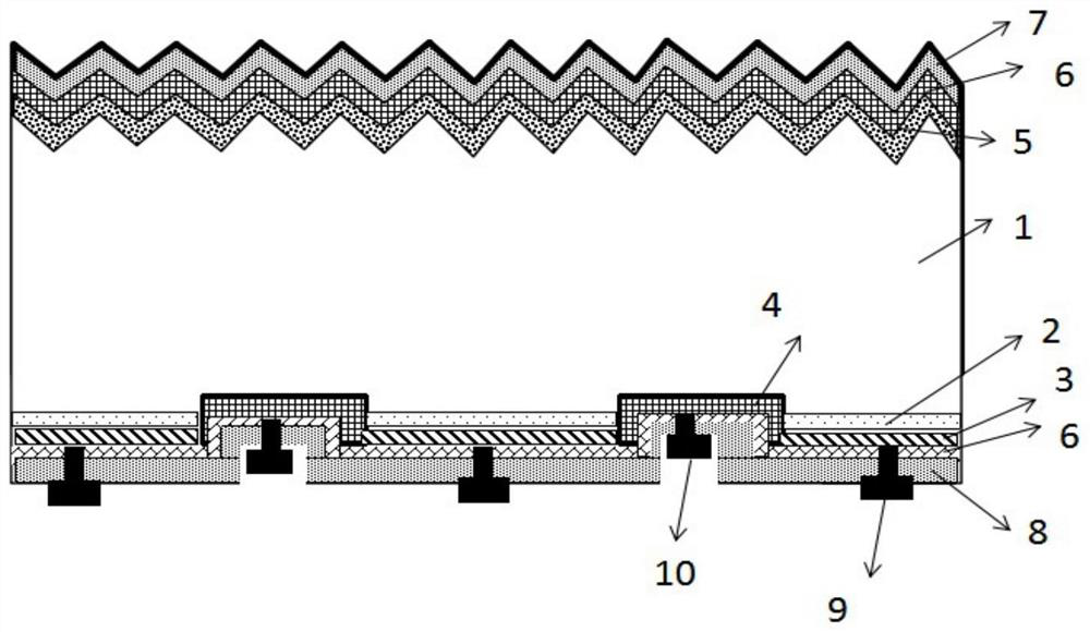
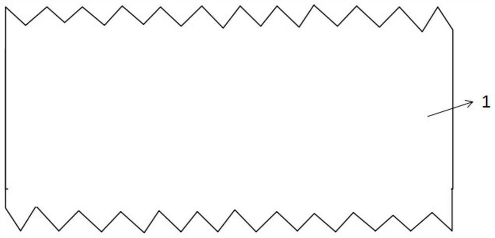
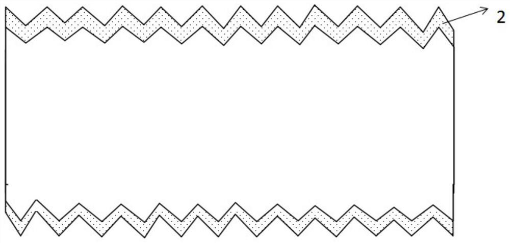
[0028] The present invention will now be described in further detail in conjunction with the accompanying drawings and preferred embodiments. These drawings are all simplified schematic diagrams, which only illustrate the basic structure of the present invention in a schematic manner, so they only show the configurations related to the present invention.

[0029] Full back electrode contact crystalline silicon photovoltaic cell (IBC cell) is a technology that moves both the positive and negative metal contacts to the back of the cell, so that the front of the cell facing the sun is completely black, and the front of most photovoltaic cells is completely invisible. metal wire. This not only brings more effective power generation area to users, but also helps to improve power generation efficiency, and the appearance is also more beautiful.

[0030] The present invention makes full use of the existing PERC equipment, and makes it into a P-type heterojunction full back electrode...


PUM

PropertyMeasurementUnit
thicknessaaaaaaaaaa
thicknessaaaaaaaaaa
thicknessaaaaaaaaaa

Abstract

The invention relates to a preparation method of a P-type heterojunction full-back electrode contact crystalline silicon photovoltaic cell, which comprises the steps of performing double-sided texturing to form a textured structure; performing double-sided oxidation and intrinsic polycrystalline silicon, and then performing phosphorus diffusion to form a tunneling oxidation passivation layer; forming a mask layer on the back surface by using a high-temperature oxidation process; carrying out laser film opening and cleaning on the back surface, and removing intrinsic polycrystalline silicon onthe front surface by utilizing an alkali polishing process; performing boron slurry printing on the back surface, and drying to form a P+ layer; forming a P+ layer on the front surface by adopting boron source doping; removing a BSG mask layer and a PSG mask layer by using HF; removing the redundant polycrystalline silicon layer in an alkali polishing manner; forming a passivation layer from double-sided aluminum oxide, front silicon oxynitride and back silicon nitride; carrying out silk-screen printing to form P+finger and N+finger; and conducting a low-temperature sintering process to complete manufacturing of the cell. According to the invention, the structure of an IBC cell is introduced on the basis of the existing PERC technology, and meanwhile, the structure of the intrinsic amorphous silicon is introduced, so that VOC and ISC can be effectively improved, and the efficiency is greatly improved.

Description

technical field [0001] The invention relates to the technical field of solar cells, in particular to a method for preparing a p-type heterojunction full-back electrode-contact crystalline silicon photovoltaic cell. Background technique [0002] The IBC (Interdigitated back contact) battery appeared in the 1970s and was the earliest researched back-junction battery. It was mainly used in concentrating systems at first. The battery uses an n-type substrate material, and the front and rear surfaces are covered with a layer of thermal oxide film to reduce surface recombination. Using photolithography technology, local diffusion of phosphorus and boron is carried out on the back of the battery respectively, forming a P region and an N region arranged in a finger-like intersecting manner, and a P+ region and an N+ region located above it. The P+ and N+ regions formed by re-expansion can effectively eliminate the voltage saturation effect under high concentration conditions. In a...

Claims


Application Information

Patent Timeline
Patent Type & Authority Applications(China)
IPC IPC(8): H01L31/18H01L31/0747H01L31/0224H01L31/0216
CPCH01L31/02167H01L31/022458H01L31/0747H01L31/1804Y02E10/547Y02P70/50
Inventor 瞿辉曹玉甲王芹芹
Owner JIANGSU SHUNFENG PHOTOVOLTAIC TECH CO LTD
Why Eureka
Try Eureka