Composition for packaging optoelectronic device, packaging structure and optoelectronic device

A technology of optoelectronic devices and packaging structures, which is applied in the direction of electric solid state devices, photovoltaic power generation, electrical components, etc., to achieve the effects of high light transmittance, high curing rate, and high heat resistance

Active Publication Date: 2020-11-13
XIAN SMART MATERIALS CO LTD
View PDF5 Cites 7 Cited by
  • Summary
  • Abstract
  • Description
  • Claims
  • Application Information

AI Technical Summary

Problems solved by technology

The current system does not meet the above requirements

Method used


Image

  • Composition for packaging optoelectronic device, packaging structure and optoelectronic device
  • Composition for packaging optoelectronic device, packaging structure and optoelectronic device
  • Composition for packaging optoelectronic device, packaging structure and optoelectronic device

Examples


Embodiment 1

[0076] Embodiment 1: Preparation of Encapsulation Composition 1

[0077] The components used are described below:

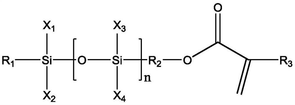
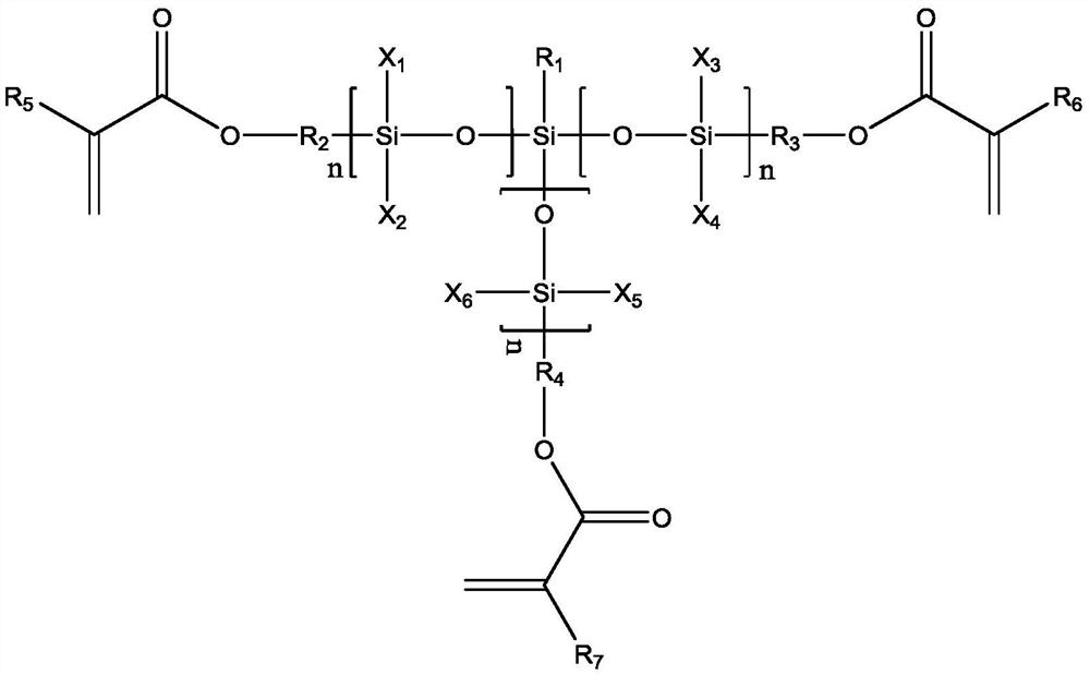
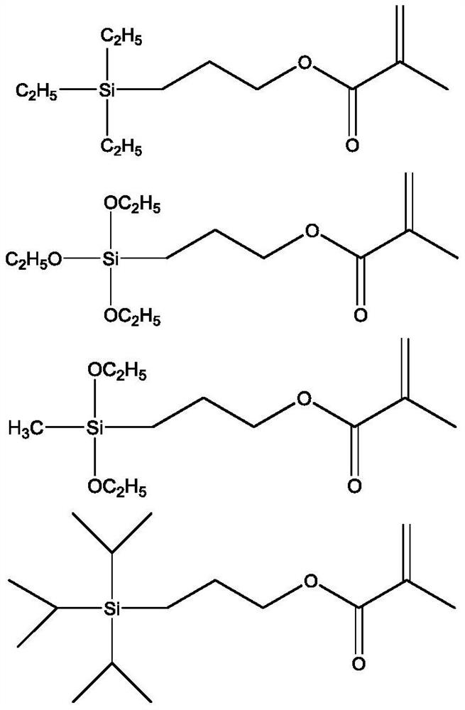
[0078] (A) silicon-containing monomer: (A1) monomer of formula 5; (A2) monomer of formula 9;

[0079] (B) Photocurable monomers: (B1) 2-phenylethyl (meth)acrylate, (B2) glycerol diacrylate;

[0080] (C) Initiator: benzyl(diphenyl)phosphine oxide.

[0081] In a brown glass bottle, add 10% (A1), 40% (B1), 45% (B2) and 5% (C) of the total mass, shake and mix at room temperature for 2 hours, and then filter to obtain the composition for packaging 1; Then apply the composition on the surface of the ITO substrate by inkjet printing to form a sample with an area size of 10cm×10cm×10um (length×width×thickness), and then pass 100mW / cm 2 The UV curing equipment cures the packaging composition by ultraviolet curing for 10 to 30 seconds, and finally forms a packaging protective film.

[0082] The performance evaluation of the encapsulant is as follows:

[0083] Photocur...

Embodiment 2

[0091] Embodiment 2: Preparation of encapsulation composition 2

[0092] A detailed description of the components used in Example 2 follows:

[0093] (A) silicon-containing monomer: (A1) monomer of formula 5; (A2) monomer of formula 9;

[0094] (B) Photocurable monomers: (B1) 2-phenylethyl (meth)acrylate, (B2) glycerol diacrylate;

[0095] (C) Initiator: benzyl(diphenyl)phosphine oxide.

[0096] In a brown glass bottle, add 10% (A2), 40% (B1), 20% (B2) and 5% (C) of the total mass, shake and mix at room temperature for 2 hours, and then filter to obtain the composition for packaging 2; Then apply the composition on the surface of the ITO substrate by inkjet printing to form a sample with an area size of 10cm×10cm×10um (length×width×thickness), and then pass 100mW / cm 2The UV curing equipment cures the packaging composition by ultraviolet curing for 10 to 30 seconds, and finally forms a packaging protective film.

Embodiment 3

[0097] Embodiment 3: Preparation of encapsulation composition 3

[0098] The components used in Example 3 are described in detail as follows:

[0099] (A) silicon-containing monomer: (A1) monomer of formula 5; (A2) monomer of formula 9;

[0100] (B) Photocurable monomers: (B1) 2-phenylethyl (meth)acrylate, (B2) glycerol diacrylate;

[0101] (C) Initiator: benzyl(diphenyl)phosphine oxide.

[0102] In a brown glass bottle, add 70% (A1), 5% (B1), 25% (B2) and 5% (C) of the total mass, shake and mix at room temperature for 2 hours, and then filter to obtain the composition for packaging 3; Then apply the composition on the surface of the ITO substrate by inkjet printing to form a sample with an area size of 10cm×10cm×10um (length×width×thickness), and then pass 100mW / cm 2 The UV curing equipment cures the packaging composition by ultraviolet curing for 10 to 30 seconds, and finally forms a packaging protective film.


PUM

PropertyMeasurementUnit
transmittivityaaaaaaaaaa

Abstract

The invention discloses a composition for packaging an optoelectronic device, a packaging structure and the optoelectronic device. The composition comprises 10%-70% of a photocurable monomer, 10%-70%of a monofunctional or trifunctional silicon-containing monomer; and 0.5%-10% of an initiator, using a silicon-containing monomer, on one hand, due to the fact that the deformation capacity of a Si-O-Si chain segment of the silicon-containing monomer is high, when the composition is impacted by force, the silicon-containing monomer can play a role in stress dispersion, internal stress is reduced,and the mechanical property of the organic packaging composition is improved; on the other hand, the thermal performance and the hydrophobic performance of the organic packaging composition can be effectively improved, and the service life of the device can be effectively prolonged when the organic packaging composition is used for thin film packaging of photoelectronic devices.

Description

technical field [0001] The invention belongs to the technical field of organic thin films, and in particular relates to a composition for packaging an optoelectronic device, a packaging structure and an optoelectronic device. Background technique [0002] With the development of science and technology, the upgrading of electronic products is also changing with each passing day, and many display devices have also changed from bulky and rigid to light and thin, foldable and bendable. Part of the performance and life of the display device is determined by its own characteristics, and the other part is guaranteed and extended by the external packaging protection. In the traditional packaging technology, the substrates used are rigid materials (such as: steel plate, acrylic, glass, ceramics and other hard materials), which lack flexibility and cannot fully meet the market demand. [0003] In Barix's Thin Film Encapsulation Technology (TFE), the inorganic barrier film will have d...

Claims


Application Information

Patent Timeline
Patent Type & Authority Applications(China)
IPC IPC(8): H01L51/54H01L51/52H01L51/50H01L51/00H01L31/048C08F222/20C08F220/18C08F230/08
CPCH01L31/0481C08F222/102H10K85/40H10K50/00H10K50/8445H10K50/84H10K50/844C08F220/18C08F230/085Y02E10/50H10K30/88
Inventor 吴朝新雷霆李璐周桂江刘育红
Owner XIAN SMART MATERIALS CO LTD
Why Eureka
Try Eureka