Nanoneedle array and its preparation method and application

A nano-needle and array technology, applied in the field of nano-needle array and its preparation, can solve the problems of difficult adjustment of nano-pillar size parameters, limited size of nano-needle array, difficulty in mass production, etc., and achieves large aspect ratio, stable related parameters, Efficient effect

Active Publication Date: 2021-06-29
深圳市安瑞生物科技有限公司
View PDF7 Cites 0 Cited by
  • Summary
  • Abstract
  • Description
  • Claims
  • Application Information

AI Technical Summary

Problems solved by technology

[0009] The purpose of the present invention is to overcome the above-mentioned deficiencies of the prior art, and provide a nanoneedle array and its preparation method, aiming at solving the existing problems in the existing nanoneedle array preparation method that the size parameters of nanopillars are difficult to adjust, the preparation area is small, and the mass production is difficult. , the technical problems of etching and growing nanoneedle arrays with limited size and poor controllability

Method used


Image

  • Nanoneedle array and its preparation method and application
  • Nanoneedle array and its preparation method and application
  • Nanoneedle array and its preparation method and application

Examples


preparation example Construction

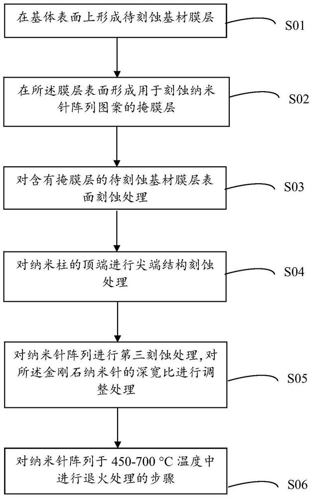
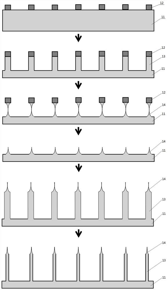
[0040] On the one hand, the embodiment of the present invention provides a method for preparing a nanoneedle array. The process flow of the preparation method of the nanoneedle array is as follows: figure 1 and figure 2 As shown, it includes the following steps:

[0041] S01: forming a substrate film layer 11 to be etched on the surface of the substrate 01;

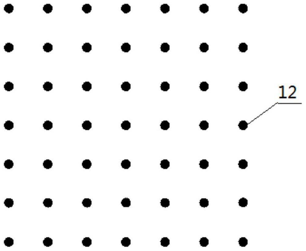
[0042] S02: forming a mask layer 12 for etching nanoneedle array patterns on the surface of the substrate film layer 11 to be etched away from the substrate;

[0043] S03. Etching treatment on the surface of the substrate film layer 11 to be etched containing the mask layer 12: from the direction of the mask layer 12 to the substrate 01, to the substrate film layer 11 formed with the mask layer 12 Etching the surface of the substrate film layer 11 to perform a first etching treatment to form a nano-column array;

[0044] S04. Carrying out the etching treatment of the tip structure 14 on the top of the nanocolumn: per...

Embodiment 1

[0082] This embodiment provides a diamond nanoneedle array and a preparation method thereof. The process flow of the diamond nanoneedle array preparation method is as follows: figure 1 and 2 , which includes the following steps:

[0083] S11. Depositing a diamond film layer 11 on the substrate surface by microwave plasma chemical vapor deposition:

[0084] a. Substrate 01 pretreatment: The monocrystalline silicon substrate was ultrasonically cleaned in acetone and alcohol for 10 min, and then washed with H 2 o 2 : NH 3 OH: H 2 O (10:10:50) solution was heated to 80 °C for 10 min, and deionized water was ultrasonically cleaned for 10 min; then the cleaned silicon substrate was placed in a stable suspension of nano-diamond powder for 1 h, and the diamond The average particle size of the powder suspension is 5 nm, it exists in the most dispersed form, the Zeta potential is about +50 mV, and the diamond nucleation density exceeds 10 11 cm -2 ;

[0085] b. Deposit the dia...

Embodiment 2

[0097] This embodiment provides a diamond nanoneedle array and a preparation method thereof. The process flow of the diamond nanoneedle array preparation method is as follows: figure 1 and 2 , which includes the following steps:

[0098] S11. Depositing a diamond film layer 11 on the substrate surface by microwave plasma chemical vapor deposition:

[0099] a. Substrate 01 pretreatment: carry out with reference to step a in step S11 of embodiment 1;

[0100]b. Depositing a diamond film layer 11 on the substrate: carry out with reference to step b in step S11 of embodiment 1;

[0101] S12. Polishing the diamond film layer 11:

[0102] Carry out with reference to step S12 of embodiment 1;

[0103] S13. Forming the mask layer 12 by electron beam lithography:

[0104] In order to promote the adhesion between the E-beam resistor and the substrate, 10 nm of Ti was evaporated onto the diamond film substrate; then the high-resolution E-beam resist HSQ was spin-coated on the subst...


PUM

PropertyMeasurementUnit
diameteraaaaaaaaaa
diameteraaaaaaaaaa
lengthaaaaaaaaaa

Abstract

The invention provides a nano-needle array and a preparation method and application thereof. The nanoneedle array preparation method of the present invention includes the following steps: forming a substrate film layer to be etched on the surface of the substrate; forming a mask layer for etching the nanoneedle array on the surface of the substrate film layer to be etched; In the direction from the mask layer to the substrate, a first etching process is performed on the surface of the film layer of the substrate to be etched on which the mask layer is formed to form a nano-column array; The top of the nano-column is subjected to a second etching process, and a tip structure is formed on the top of the nano-column to form a nano-needle array. The nano-needles contained in the nano-needle array include a nano-needle body, and the needle head of the nano-needle body is a tip structure.

Description

technical field [0001] The invention belongs to the technical field of micro-nano biochip manufacturing, and in particular relates to a nano-needle array and its preparation method and application. Background technique [0002] Diamond is a multifunctional material with unique properties, integrating extreme physical and chemical properties such as electricity, optics, mechanics, and heat. In addition to the inherent physical and chemical properties of diamond, one-dimensional nano-diamonds also have some properties that bulk diamonds do not have due to changes in their shape and size, such as hard and elastic mechanical properties, high specific surface area, and tip effect. Wait. Therefore, one-dimensional nanodiamond arrays have important applications in many fields such as drug delivery, chemical and biological sensors, high-performance electrodes, analytical sensors, and quantum information devices. [0003] The technology of using high aspect ratio nanomaterials to m...

Claims


Application Information

Patent Timeline
Patent Type & Authority Patents(China)
IPC IPC(8): B81C1/00B81B1/00A61M37/00
CPCA61M37/0015A61M2037/0053A61M2037/0061B81B1/008B81C1/00031B81C1/00111B81C1/00531
Inventor 杨扬史鹏张文军
Owner 深圳市安瑞生物科技有限公司
Why Eureka
Try Eureka