Substrate wafer structure for improving resistivity of substrate and preparation method

A substrate wafer and resistivity technology, which is applied in the manufacture of circuits, electrical components, semiconductors/solid-state devices, etc., can solve the problem that the power consumption of low-power devices cannot be effectively reduced significantly, and the thickness of the substrate cannot be effectively thinned , Improve resistivity and other issues, achieve the effect of improving resistivity, solving technical requirements for ultra-thin sheet processing, and increasing the range of resistivity

Inactive Publication Date: 2020-11-20
HUNAN UNIV
View PDF4 Cites 0 Cited by
  • Summary
  • Abstract
  • Description
  • Claims
  • Application Information

AI Technical Summary

Problems solved by technology

For Si MOSFET, a low-power device with a vertical conductive structure, with the update and iteration of technology, its conversion efficiency is constantly improving, and its power density is also rising, which leads to the increasing proportion of substrate resistance in the total resistance of the device. Due to the limitation of traditional Semiconductor substrate thinning process, the thickness of the substrate cannot be effectively reduced, and the bottleneck of power consumption of low-power devices cannot be effectively and greatly reduced
In addition, the polished wafers provided by wafer suppliers are prepared by the Czochralski process. For silicon N-type polished wafers, which are uniformly doped, the resistivity is generally 0.0006-0.0007Ω·cm. Limitation, can not achieve very high doping concentration to improve resistivity
In summary, the large proportion of substrate resistance has become a key bottleneck in the sustainable development of low-power devices with silicon-based vertical conductive structures in achieving high conversion efficiency and high power density.

Method used


Image

  • Substrate wafer structure for improving resistivity of substrate and preparation method
  • Substrate wafer structure for improving resistivity of substrate and preparation method
  • Substrate wafer structure for improving resistivity of substrate and preparation method

Examples


Embodiment Construction

[0041] The following will clearly and completely describe the technical solutions in the embodiments of the present invention with reference to the accompanying drawings in the embodiments of the present invention. Obviously, the described embodiments are only some, not all, embodiments of the present invention. Based on the embodiments of the present invention, all other embodiments obtained by persons of ordinary skill in the art without making creative efforts belong to the protection scope of the present invention.

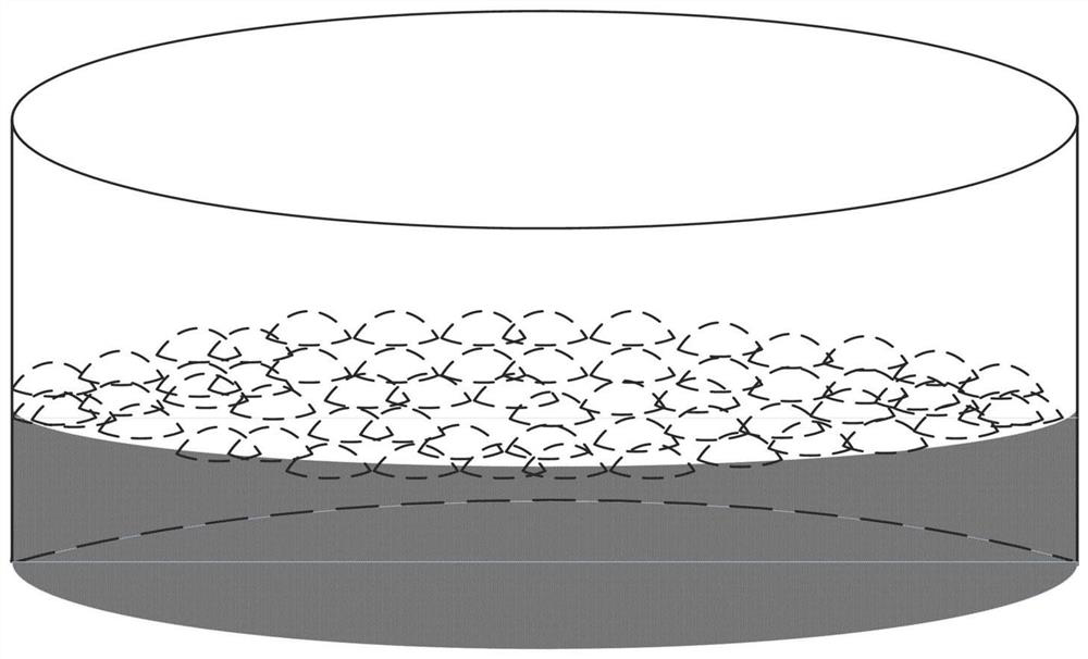
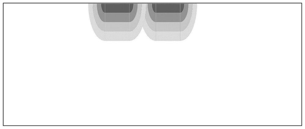
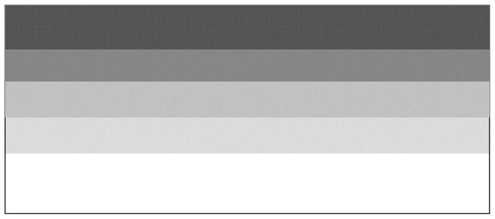
[0042] combined with figure 2 And attached image 3 The schematic diagram of the substrate structure of the single-sided ion implantation or doping method under different implantation windows and depths, the distribution of the ion structure inside the wafer after high temperature diffusion is shown in the attached figure 1 shown;

[0043] Step 1: Select a certain amount of substrate wafers and divide them into different intervals according to different res...


PUM


Abstract

The invention discloses a substrate wafer structure for improving the resistivity of a substrate and a preparation method, and relates to a semiconductor substrate wafer. The method comprises the following steps of: dividing the substrate wafer into different resistivity ranges according to the substrate wafer provided by a wafer manufacturer; selecting substrate wafers with different resistivityranges, carrying out ion implantation or doping, and forming a high-concentration surface area in a certain window range of the surface. The implanted or doped ions exist below the surface of the window in the form of Gaussian distribution, and a three-dimensional wafer structure formed by high-temperature diffusion forms a corresponding relation table of different implanted or doped windows and implanted or doped depths and reduced resistivity percentages through multiple experiments. In resistivity improvement of the substrate wafer later, the resistivity of the substrate wafer is optimizedeffectively and precisely according to the corresponding relation table. The practicability is high, the control scheme is good, the effect is obvious, the performance is greatly improved, meanwhile,the requirements of users are greatly met, the manufacturing cost is reduced, and the current process conditions are met.

Description

technical field [0001] The invention relates to a semiconductor substrate, in particular to a wafer structure and a process preparation method for improving the resistivity of a power device substrate. Background technique [0002] The main raw materials for the manufacture of power semiconductor devices are single crystal epitaxial wafers and single crystal polished wafers. Single crystal polished wafers are the substrate layer, which mainly play a supporting role in the process of epitaxial growth and device manufacturing. Layers are used in the fabrication of devices. In the manufacture of silicon-based devices, due to the hard and brittle properties of silicon materials, a certain thickness is required in both the single crystal epitaxial wafer and the substrate to increase its strength, which is sufficient to support the operation of device preparation. [0003] Silicon-based devices have sufficiently thick substrates, resulting in a large proportion of substrate resis...

Claims


Application Information

Patent Timeline
IPC IPC(8): H01L29/06H01L21/22H01L21/265H01L21/324
CPCH01L21/22H01L21/265H01L21/324H01L29/06H01L29/0684H01L29/0688
Inventor 王俊俞恒裕
Owner HUNAN UNIV
Why Eureka
Try Eureka