SOI lateral insulated gate bipolar transistor

A technology of bipolar transistors and insulated gates, applied in semiconductor devices, electrical components, circuits, etc., can solve the problems that limit the application of ordinary anode short-circuit structure IGBT devices, etc., to reduce the current conduction path, increase the saturation current, and forward voltage drop Reduced effect

Active Publication Date: 2020-11-20
UNIV OF ELECTRONICS SCI & TECH OF CHINA +1
View PDF8 Cites 6 Cited by
  • Summary
  • Abstract
  • Description
  • Claims
  • Application Information

AI Technical Summary

Problems solved by technology

But at the same time, the introduction of anode N+ makes the device switch from unipolar conduction mode to bipolar conduction mode, there is a Snapback phenomenon (the I-V curve is roundabout and presents a negative resistance state), such instability limits the application of ordinary anode short-circuit structure IGBT devices

Method used


Image

  • SOI lateral insulated gate bipolar transistor
  • SOI lateral insulated gate bipolar transistor
  • SOI lateral insulated gate bipolar transistor

Examples


Embodiment 1

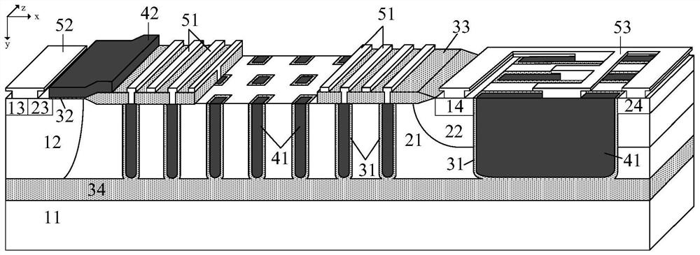
[0032] A lateral insulated gate bipolar transistor device described in Embodiment 1, such as figure 1 and figure 2 shown, including:

[0033] First conductivity type semiconductor substrate 11, first conductivity type well region 12, first conductivity type heavily doped emitter region 13, first conductivity type heavily doped collector region 14, second conductivity type drift region 21, Two conductive type well region 22 , second conductive type heavily doped emitter region 23 , second conductive type heavily doped collector region 24 , first dielectric oxide layer 31 , second dielectric oxide layer 32 , third dielectric oxide layer 33, buried oxide layer 34, polysilicon electrode 41, control gate polysilicon electrode 42, metal strip 51, emitter contact electrode 52, collector contact electrode 53;

[0034] The buried oxide layer 34 is located above the first conductive type semiconductor substrate 11 , the second conductive type drift region 21 is located above the buri...

Embodiment 2

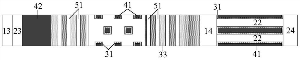
[0046] like image 3 As shown, it is a schematic structural diagram of the SOI lateral insulated gate bipolar transistor of Embodiment 2. The difference between the structure of this embodiment and Embodiment 1 is that the distribution of the vertical field plates in the collector region is different. In this embodiment, the adjacent two The interval between the column longitudinal field plates is reduced, and the length of the field plates is shortened to reach the anode resistance size that can eliminate the Snapback effect. The working principle is basically the same as that of the first embodiment.

Embodiment 3

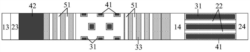
[0048] like Figure 4 As shown, it is a top view of the SOI lateral insulated gate bipolar transistor structure of Embodiment 3. The difference between the structure of this embodiment and Embodiment 1 is that by reducing the width of the etched deep groove, the oxide layer in the later oxidation process of the groove wall is reduced. Filling the trench completely, the collector region longitudinal field plate becomes a dielectric trench. Adjust the interval of the medium tank to obtain a suitable anode resistance size to eliminate the Snapback effect. The working principle is basically the same as that of Example 1.


PUM


Abstract

The invention provides an SOI transverse insulated gate bipolar transistor, which is characterized in that a first dielectric oxide layer and a floating field plate polycrystalline silicon electrode form a longitudinal floating field plate which is distributed in a whole second conduction type drift region to form a longitudinal floating field plate array; and a longitudinal field plate connectedwith the collector contact electrode is formed in the collector region by the same process, and a second conductive type well region is inserted in parallel to form an anode resistance structure. Whenthe transistor is in an on state, an accumulation layer can be formed on the surface of the longitudinal floating field plate, and the saturation current of the device is improved. The longitudinal field plate introduced into the well region of the second conductive type can accurately control the size of the anode resistance, eliminates the impact on the output characteristics of the device fromthe snapback phenomenon, and improves the stability of the device.

Description

technical field [0001] The invention belongs to the field of power semiconductors, and mainly provides an SOI lateral insulated gate bipolar transistor. Background technique [0002] Lateral insulated gate bipolar transistors have the advantages of high input impedance, voltage control, and low on-resistance, and have the advantage of ease of integration that vertical devices do not have. Therefore, the lateral insulated gate bipolar transistor is more and more valued and respected, so that the development is more rapid and the application field is more and more extensive. When the conventional lateral insulated gate bipolar transistor is turned on, holes are injected into the drift region, resulting in a conductance modulation effect, resulting in a larger current density. When turned off, a large number of carriers in the drift region can only be eliminated by recombination, resulting in a large turn-off loss. Therefore, the anode short-circuit structure N+ is introduced...

Claims


Application Information

Patent Timeline
Patent Type & Authority Applications(China)
IPC IPC(8): H01L29/40H01L29/739
CPCH01L29/404H01L29/407H01L29/7394
Inventor 章文通朱旭晗祖健乔明李肇基张波
Owner UNIV OF ELECTRONICS SCI & TECH OF CHINA
Why Eureka
Try Eureka