Locking glue array lead frame and application thereof in chip packaging piece

A glue-locking array lead and lead frame technology, which is applied to the glue-locking array lead frame and its application in chip packages, can solve the problem of limited number of openings, unsatisfactory contact effect between bonding wire and copper material, and meaning of use There are no major problems, and the effect of improving reliability is achieved

Pending Publication Date: 2020-11-24
郑州兴航科技有限公司
View PDF9 Cites 1 Cited by
  • Summary
  • Abstract
  • Description
  • Claims
  • Application Information

AI Technical Summary

Problems solved by technology

The main body of the lead frame is made of copper, which has a good bonding ability with the plastic encapsulant, but the contact effect between the bonding wire and the copper used in the wire bonding process is not ideal, and silver plating is required on the appropriate area of ​​the lead frame
The bonding ability between the silver-plated layer and the plastic packaging compound is slightly smaller than that of copper, so the position of the silver-plated layer after product encapsulation is prone to serious plastic package separation defects, and it is difficult to meet the high reliability requirements of electronic packaging
[0003] At present, the lead frame has full plating (that is, the pin precision pressing area in the lead frame and the substrate are all silver-plated), single-ring plating (that is, only the pin precision pressing area in the lead frame is silver-plated), and double-ring plating (that is, the lead frame is silver-plated). Silver-plated inner pin precision pressing area, there is a silver-plated ri...

Method used


Image

  • Locking glue array lead frame and application thereof in chip packaging piece
  • Locking glue array lead frame and application thereof in chip packaging piece
  • Locking glue array lead frame and application thereof in chip packaging piece

Examples


Embodiment 1

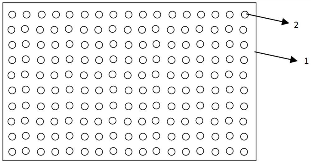
[0062] A kind of adhesive lock array lead frame of the present invention, as figure 1 As shown, the lead frame substrate 1 is rectangular, and its surface is provided with a glue-locking structure. The glue-locking structure is a circular glue-locking hole 2 evenly distributed on the lead-frame substrate. The diameter of the circular glue-locking hole 2 is 300um, the distance between the edges of two adjacent circular locking holes 2, that is, the tangent line tangent to the circle is 270um.

Embodiment 2

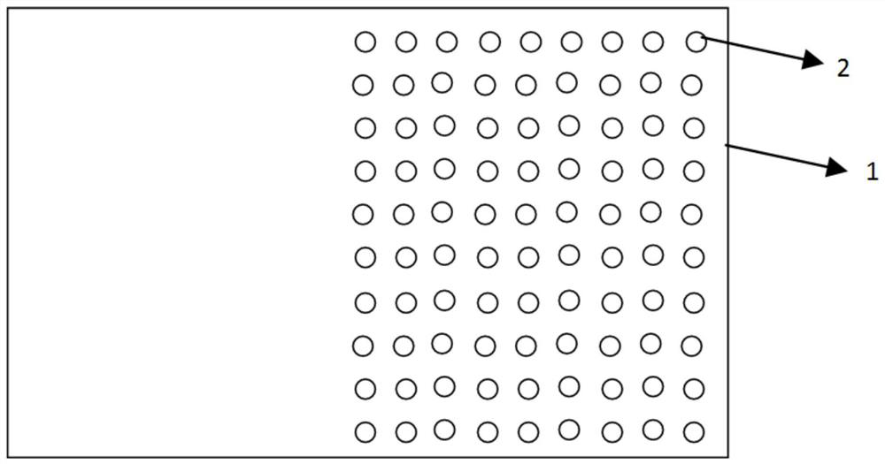
[0064] A kind of adhesive lock array lead frame of the present invention, as figure 2 As shown, the lead frame substrate 1 is rectangular, and its surface is provided with a glue-locking structure. The glue-locking structure is a circular glue-locking hole 2 distributed on half of the surface of the lead-frame substrate. The diameter is 30um, and the distance between the edges of two adjacent locking holes 2 is 207um.

Embodiment 3

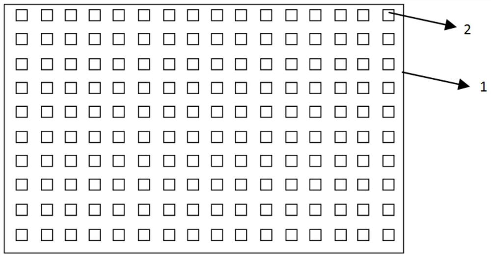
[0066] A kind of adhesive lock array lead frame of the present invention, as image 3 As shown, the lead frame substrate 1 is rectangular, and its surface is provided with a glue-locking structure. The glue-locking structure is a square glue-locking hole 2 evenly distributed on the lead-frame substrate, and the side length of the square glue-locking hole 2 is 80um. , the distance between the edges of two adjacent locking holes 2 is 400um.


PUM

PropertyMeasurementUnit
Diameteraaaaaaaaaa

Abstract

The invention discloses a locking glue array lead frame and application of the locking glue array lead frame in a chip packaging piece; a plurality of locking glue holes are uniformly formed in the surface of a substrate of the lead frame, and areas, without holes, among the locking glue holes are used for lead bonding. When the lead frame is applied, the application comprises the following steps:step 1, thinning a wafer of a chip, and then pasting a DAF film on the back surface; step 2, adhering the chip to the substrate of the lead frame; step 3, cleaning a circuit to be bonded, and carrying out lead bonding between the chip and the substrate, between the chip and pins, between the substrate and the pins, or between the chips to obtain a bonded circuit; and step 4, performing plasma cleaning on the bonded circuit, performing plastic package by a plastic package material, embedding the plastic package material into plastic locking holes to form a plastic package body, curing the plastic package body, then sequentially carrying out electrotinning, laser marking and rib cutting forming to obtain a single-chip package part. The plastic package material penetrates through the plasticlocking holes, the effects of pinning strengthening and separation layer spreading preventing are achieved, and the reliability of the product is improved.

Description

technical field [0001] The invention belongs to the field of packaging and testing of semiconductor integrated circuits, in particular to a glue-locking array lead frame and its application in chip packaging. Background technique [0002] Lead frame is one of the main basic materials for integrated circuit plastic packaging production. Its substrate carries the chip, the inner pin is connected to the chip, and the chip is connected to the external circuit through the outer pin, so as to ensure smooth power supply and signal. The main body of the lead frame is made of copper, which has a good bonding ability with the plastic encapsulant, but the contact effect between the bonding wire and the copper used in the wire bonding process is not ideal, and it is necessary to perform silver plating on the appropriate area of ​​the lead frame. The bonding ability between the silver-plated layer and the plastic packaging compound is slightly smaller than that of copper, so the position...

Claims


Application Information

Patent Timeline
IPC IPC(8): H01L23/495H01L23/31
CPCH01L23/49503H01L23/3121H01L2224/48145H01L2224/48247H01L2924/181H01L2224/48137H01L2924/19107H01L2924/00012
Inventor 方兆国周少明施英铎
Owner 郑州兴航科技有限公司
Why Eureka
Try Eureka