

A kind of abrasive liquid for semiconductor wafer processing
A wafer processing and polishing liquid technology, which is applied in the direction of sustainable manufacturing/processing, polishing compositions containing abrasives, and other chemical processes, can solve the problems of high wafer processing costs, adjusted products, and high prices, and achieve Good fluidity, improved yield rate, and stable suspension performance
Active Publication Date: 2022-06-03
中科孚迪科技发展有限公司
View PDF16 Cites 0 Cited by
- Summary
- Abstract
- Description
- Claims
- Application Information
AI Technical Summary
Problems solved by technology
However, the price of this product is very expensive, which makes the cost of wafer processing remain high. On the other hand, due to technological monopoly, the product cannot be adjusted according to the characteristics of the Chinese market and the requirements of specific processing parameters.
Method used
View moreImage
Smart ImageViewing Examples

Examples
Embodiment 1
Embodiment 2
Embodiment 3
Login to View More PUM
 Abstract
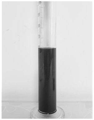
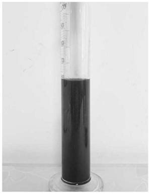
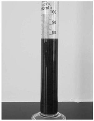
The invention discloses a grinding liquid for semiconductor wafer processing, and relates to the technical field of grinding and polishing of hard and brittle materials. The grinding liquid for semiconductor wafer processing disclosed by the invention is composed of the following components in weight percentage: 20-30% of solid abrasive, 10-20% of thickener, 3-10% of dispersant, and 3-10% of wetting agent. %, lubricant 3-10%, coupling agent 10-30%, defoamer 1-3%, solvent 10-50% and the balance is deionized water. The grinding fluid provided by the invention has stable suspension performance, the grinding agent is not easy to sink to the bottom during processing, and can be used repeatedly for multiple times; it has good fluidity, no agglomeration phenomenon, and avoids blocking the infusion pipeline; the surface wettability and dispersibility are excellent. Excellent, the abrasive liquid is evenly distributed during the processing, avoiding scratches on the processing interface, and improving the yield rate of processing; easy to clean, avoiding the introduction of impurities into the subsequent processing process, and at the same time, the grinding removal rate under the same conditions is high, improving processing efficiency.
Description
A kind of grinding liquid for semiconductor wafer processing technical field The invention belongs to the technical field of grinding and polishing processing of hard and brittle materials, in particular to a kind of processing for semiconductor wafers grinding fluid. Background technique In recent years, with the rapid development of my country's economy, the rise of electronic products such as mobile communications, the smart commodity market has With explosive growth, especially with the advent of the 5G era, the demand for various semiconductor materials continues to grow. For example, single crystal silicon can be used for Computer chips, polycrystalline silicon can be used for solar cells, gallium arsenide, indium phosphide, etc. can be used in integrated circuits, single crystal aluminum oxide can be used on the display, etc. Semiconductor materials must be processed before they are applied, and in the grinding process of semiconductors, the Grinding fluid...
Claims
Login to View More Application Information
Patent Timeline
 Patent Type & AuthorityPatents(China)
IPC IPC(8): C09G1/02C09K3/14
CPCC09G1/02C09K3/1463Y02P70/50
Inventor祁有丽南振华
Owner中科孚迪科技发展有限公司