Driving integrated circuit of SiC MOSFET switching device

A technology for driving integrated circuits and switching devices, applied in electronic switches, electrical components, pulse technology, etc., can solve problems such as breakdown damage, large circuit area, and increased switching loss

Pending Publication Date: 2020-12-04
XIDIAN UNIV
View PDF9 Cites 5 Cited by
  • Summary
  • Abstract
  • Description
  • Claims
  • Application Information

AI Technical Summary

Problems solved by technology

[0004] Takata, Yang Yan, Cheng Ze and others disclosed a silicon carbide MOSFET drive circuit in their patent application document "A Silicon Carbide MOSFET Drive Circuit" (application publication number CN108683327A, application number 201810600993.4, application date 2018.06.12), The PWM (Pulse width modulation, pulse width modulation) control circuit generates a PWM pulse signal. After the PWM pulse signal passes through the driving signal amplification circuit, it passes through the resistor to control the silicon carbide MOSFET switch. The output of the power supply includes +15V, 0V and -3V DC voltage, + The 15V and -3V DC voltages respectively supply power to the drive signal amplifier circuit, and the 0V is connected to the source of the silicon carbide MOSFET; the silicon carbide MOSFET drive circuit can reduce the upper and lower tubes of the bridge arm circuit in the power electronic converter by turning off the driving negative voltage. Crosstalk avoids the straight-through of the bridge arm and imp

Method used


Image

  • Driving integrated circuit of SiC MOSFET switching device
  • Driving integrated circuit of SiC MOSFET switching device
  • Driving integrated circuit of SiC MOSFET switching device

Examples


Embodiment 1

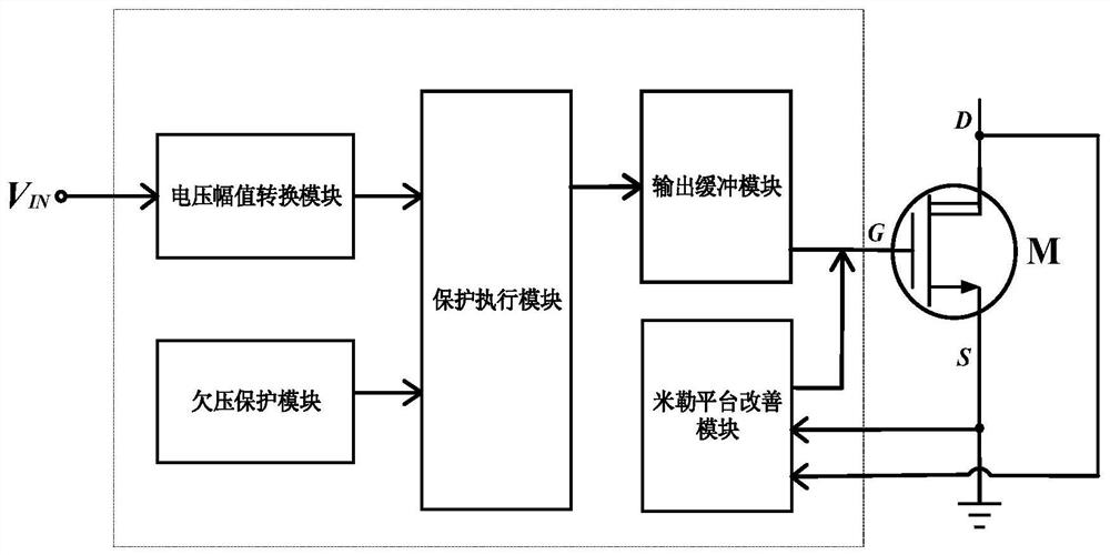
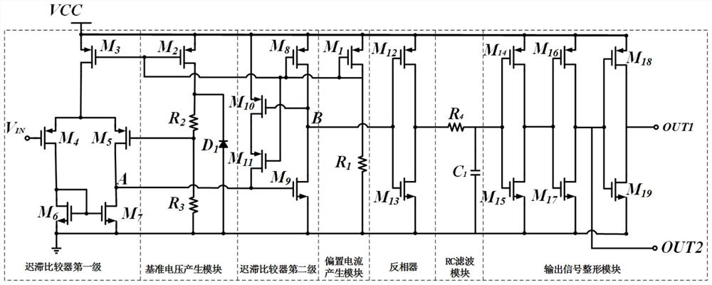
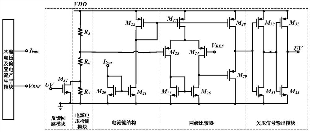
[0051] See figure 1 , figure 1 A block diagram of a driving integrated circuit for a SiC MOSFET switching device provided by an embodiment of the present invention. The driving integrated circuit of the SiC MOSFET switching device includes: a voltage amplitude conversion module, an undervoltage protection module, a protection execution module, an output buffer module and a Miller platform improvement module. in,

[0052]The input end of the voltage amplitude conversion module inputs an external input square wave signal, the output end of the voltage amplitude conversion module is connected to the first input end of the protection execution module, and the output end of the undervoltage protection module is connected to the second input end of the protection execution module. The output terminal of the protection execution module is connected to the input terminal of the output buffer module, the output terminal of the output buffer module is connected to the gate of the exte...


PUM


Abstract

The invention relates to a driving integrated circuit of a SiC MOSFET switching device. The driving integrated circuit comprises a voltage amplitude conversion module, an undervoltage protection module, a protection execution module, an output buffer module and a miller platform improvement module. According to the driving integrated circuit, a VGS platform of a power tube in a switching-on process is improved, a VDS descending speed is increased, losses are reduced, a condition that oscillation and overshoot are reduced by sacrificing a switching speed and increasing the switching losses is prevented, and meanwhile current spikes are avoided; and in addition, the driving circuit is designed into an integrated circuit so that a circuit area is greatly reduced.

Description

technical field [0001] The invention belongs to the technical field of integrated circuits, and in particular relates to a driving integrated circuit for a SiC MOSFET switching device. Background technique [0002] At present, power electronic devices are mainly based on silicon-based devices. However, due to the narrow bandgap of silicon materials, it is difficult to meet the requirements of the new generation of power systems in terms of blocking voltage, energy consumption, operating temperature and switching frequency, and has become a bottleneck in the development of power electronic systems. In order to solve this contradiction, research on third-generation semiconductor materials is developing rapidly, among which silicon carbide (SiC) material is the most promising material to replace silicon (Si) and become the material of choice for the preparation of a new generation of power semiconductor devices. SiC MOSFET (Metal-Oxide-Semiconductor Field-Effect Transistor, ox...

Claims


Application Information

Patent Timeline
IPC IPC(8): H03K17/16
CPCH03K17/165Y02B70/10
Inventor 张艺蒙周敏吕红亮汤晓燕宋庆文张玉明
Owner XIDIAN UNIV
Why Eureka
Try Eureka