Binding board thick frame printing process

A thick frame and process technology, used in printed circuits, printed circuit manufacturing, printed circuit drying, etc., can solve the problems of difficult control, product defects, and high production costs, and achieve easy control, high product reliability, and side erosion. small effect

Inactive Publication Date: 2020-12-08
东莞市高迈电子有限公司
View PDF5 Cites 0 Cited by
  • Summary
  • Abstract
  • Description
  • Claims
  • Application Information

AI Technical Summary

Problems solved by technology

[0005] In order to overcome the above-mentioned defects of the prior art, an embodiment of the present invention provides a printing process for binding plate thickness frames. The technical problem to be solved by the present invention is: it is difficult

Method used


Image

  • Binding board thick frame printing process

Examples


Embodiment 1

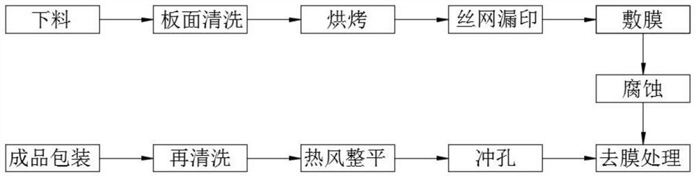
[0029] The invention provides a thick frame printing process for a binding plate, comprising the following steps:

[0030] Step S1: blanking, cutting the substrate into the desired shape to make a binding board;

[0031] Step S2: Clean the surface of the board, put the binding board into water, and use ultrasonic cleaning to clean the surface to remove surface residues;

[0032] Step S3: Bake, bake the cleaned binding board in a nitrogen-filled oven at a temperature of 155°C for 40 minutes, and dry it with water to avoid explosion and shrinkage;

[0033] Step S4: screen printing, print the required circuit diagram on the binding board through screen printing lead-free solder paste, use lead-free solder with a composition of 96.5Sn / 3.5Ag, which has the characteristics of high strength and high melting point , the viscosity is controlled at 770,000 CPS, and screen printing is performed at room temperature;

[0034] Step S5: apply a film, apply a protective film of the circuit ...

Embodiment 2

[0042] The invention provides a thick frame printing process for a binding plate, comprising the following steps:

[0043] Step S1: blanking, cutting the substrate into the desired shape to make a binding board;

[0044] Step S2: Clean the surface of the board, put the binding board into water, and clean it by ultrasonic cleaning;

[0045] Step S3: Bake, bake the cleaned binding board in a nitrogen-filled oven at a temperature of 145°C for 40 minutes, and dry it with water;

[0046] Step S4: screen printing, print the required circuit diagram on the binding board through screen printing lead-free solder paste, use lead-free solder with a composition of 95.5Sn / 3.5 / Ag / 1Zn, and control the viscosity at 770,000 CPS, screen printing at room temperature;

[0047] Step S5: apply a film, apply a protective film of the circuit diagram on the binding board, and prepare for corrosion;

[0048] Step S6: Corrosion, spraying the etching solution into a spray on the previously processed b...


PUM


Abstract

The invention discloses a binding board thick frame printing process, and particularly relates to the technical field of circuit board printing, the binding board thick frame printing process comprises the following steps: S1, blanking, specifically, cutting a substrate into a required shape to prepare a binding board; s2, plate surface cleaning, specifically, putting the binding board into water,and cleaning the binding board in an ultrasonic cleaning mode; s3, baking, specifically, bakingthe cleaned binding board, and drying water; s4, silk screen skip printing, specifically, printing a required circuit diagram on the binding board through silk screen skip printing lead-free solder paste; and S5, coating, specifically, coating the binding board with a circuit diagram protection film, and preparing for corrosion. According to the circuit board printing process, printing is conducted on the binding board, board explosion and expansion and contraction are avoided through cleaning and drying, corrosion is achieved through spraying of spray heads, control is easy, lateral corrosion is small, the binding board can be effectively protected through hot air leveling, flaws are avoided when the high-precision circuit board is produced, the product reliability is high, and the production cost can be controlled at the normal level.

Description

technical field [0001] The present invention relates to the technical field of circuit board printing, and more specifically, the present invention relates to a printing process of a thick frame of a binding board. Background technique [0002] Printed circuit board rigid board, flexible board and soft-rigid circuit board have complex structures, including single-layer, double-layer or even multi-layer. The more layers, the more complicated the process, and the printing process is also different. The electrical connection of electronic components, the circuit formed by connecting with ordinary wires has the advantages of small size, simple assembly process, high installation efficiency, and high circuit reliability, providing a good development space for the integration, miniaturization, and automation of production of electronic equipment , Widely used in electronic computers, communications, aerospace and home appliances and other industries. [0003] It is difficult to c...

Claims


Application Information

Patent Timeline
IPC IPC(8): H05K3/12H05K3/22H05K3/26H05K3/00
CPCH05K3/0085H05K3/1225H05K3/227H05K3/26H05K2203/0736H05K2203/1105H05K2203/111
Inventor 蒋文静
Owner 东莞市高迈电子有限公司
Why Eureka
Try Eureka