LED apparatus and evaporation method thereof
An evaporation and device technology, applied in the field of OLED, can solve the problems of collision quenching, reduction of lifespan reduction efficiency, etc., to achieve the effect of improving device efficiency, improving device lifespan, and consistent light emitting direction
- Summary
- Abstract
- Description
- Claims
- Application Information
AI Technical Summary
Problems solved by technology
Method used
Image
Examples
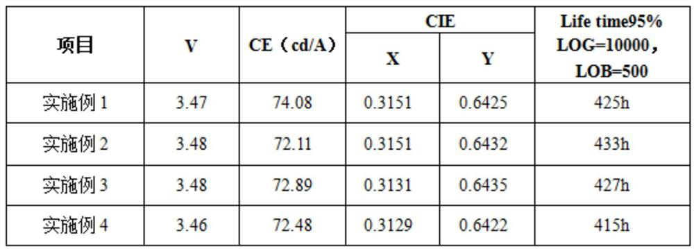
Embodiment 1
[0028] A kind of OLED device, its layer structure comprises successively stacked ITO anode, hole injection layer, hole transport layer, electron blocking layer, light-emitting layer, electron transport layer, electron injection layer, Ag cathode from top to bottom, this OLED device The evaporation method comprises the following process steps:
[0029] 1) Pre-treatment of the ITO substrate by evaporation: The ITO substrate is scrubbed with cleaning solution, ultrasonically cleaned with cleaning solution and ultrasonically cleaned with pure water three times, then baked, and placed in a vacuum sampling chamber to evacuate to a vacuum The speed is 5.0E-0.4Pa, and the rotation speed of the rotating tray is 5r / min;
[0030] 2) Place the pretreated ITO substrate in the evaporation chamber, control the vacuum degree in the evaporation chamber to 2.0E-5Pa, and stack the evaporated hole injection layer, hole transport layer, and electron blocking layer on the ITO substrate in sequence....
Embodiment 2
[0034] A kind of OLED device, its layer structure comprises successively stacked ITO anode, hole injection layer, hole transport layer, electron blocking layer, light-emitting layer, electron transport layer, electron injection layer, Ag cathode from top to bottom, this OLED device The evaporation method comprises the following process steps:
[0035] 1) Pre-treatment of the ITO substrate by evaporation: The ITO substrate is scrubbed with cleaning solution, ultrasonically cleaned with cleaning solution and ultrasonically cleaned with pure water three times, then baked, and placed in a vacuum sampling chamber to evacuate to a vacuum The speed is 3.0E-0.4Pa, and the rotation speed of the rotating tray is 12r / min;
[0036] 2) Place the pretreated ITO substrate in the evaporation chamber, control the vacuum degree in the evaporation chamber to 4.0E-5Pa, and stack the evaporated hole injection layer, hole transport layer, and electron blocking layer on the ITO substrate in sequence...
Embodiment 3
[0040] A kind of OLED device, its layer structure comprises successively stacked ITO anode, hole injection layer, hole transport layer, electron blocking layer, light-emitting layer, electron transport layer, electron injection layer, Ag cathode from top to bottom, this OLED device The evaporation method comprises the following process steps:
[0041] 1) Pre-treatment of the ITO substrate by evaporation: The ITO substrate is scrubbed with cleaning solution, ultrasonically cleaned with cleaning solution and ultrasonically cleaned with pure water three times, then baked, and placed in a vacuum sampling chamber to evacuate to a vacuum The speed is 4.0E-0.4Pa, and the rotation speed of the rotating tray is 12r / min;
[0042] 2) Place the pretreated ITO substrate in the evaporation chamber, control the vacuum degree in the evaporation chamber to 3.0E-5Pa, and stack the evaporated hole injection layer, hole transport layer, and electron blocking layer on the ITO substrate in sequence...
PUM
 Abstract
Description
Claims
Application Information


