
No-snapback silicon-controlled rectifier type ESD protection structure and implementation method thereof

An ESD protection and silicon-controlled rectifier technology, which is applied in the manufacture of electrical solid-state devices, semiconductor devices, and semiconductor/solid-state devices, etc., can solve the problems of reduced layout area and small secondary breakdown current, and achieve the effect of saving layout area.

Pending Publication Date: 2020-12-22
SHANGHAI HUALI MICROELECTRONICS CORP
View PDF0 Cites 0 Cited by
  • Summary
  • Abstract
  • Description
  • Claims
  • Application Information

AI Technical Summary

Problems solved by technology

The low-voltage PMOS device is a common electrostatic protection device without hysteresis effect, because the parasitic PNP transistor current gain is relatively small when the hysteresis effect occurs, but the shortcoming of the low-voltage PMOS device is the secondary breakdown of the hysteresis effect The current (It2) is relatively small, so the industry has been researching and developing an anti-static protection device that has no hysteresis effect and has a high secondary breakdown current.
[0008] Although Figure 4 The new non-hysteresis effect silicon-controlled rectifier type ESD protection structure removes the left shallow trench isolation layer (STI, Shallow Trench Isolation) 10 and high-concentration N-type doping (N+) 30 to reduce the layout area, but with The trend of device miniaturization puts forward higher layout area requirements, and the layout area of ​​the silicon-controlled rectifier without hysteresis effect has a technical requirement for further reduction

Method used


Image

  • No-snapback silicon-controlled rectifier type ESD protection structure and implementation method thereof
  • No-snapback silicon-controlled rectifier type ESD protection structure and implementation method thereof
  • No-snapback silicon-controlled rectifier type ESD protection structure and implementation method thereof

Examples


Embodiment Construction

[0036] The implementation of the present invention is described below through specific examples and in conjunction with the accompanying drawings, and those skilled in the art can easily understand other advantages and effects of the present invention from the content disclosed in this specification. The present invention can also be implemented or applied through other different specific examples, and various modifications and changes can be made to the details in this specification based on different viewpoints and applications without departing from the spirit of the present invention.

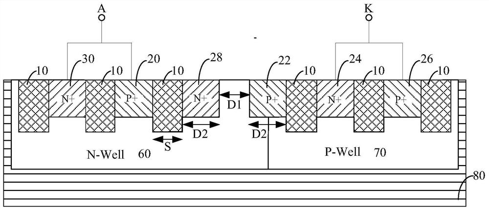
[0037] Figure 5 It is a circuit structure diagram of a preferred embodiment of a silicon-controlled rectifier type ESD protection structure without hysteresis effect in the present invention. Such as Figure 5 As shown, the present invention discloses a silicon-controlled rectifier type ESD protection structure without hysteresis effect, including a plurality of shallow trench isolation l...


PUM


Abstract

The invention discloses a no-snapback silicon-controlled rectifier type ESD protection structure and an implementation method thereof. The structure comprises a semiconductor substrate (80) and an N well (60) and a P well (70) generated on the semiconductor substrate, a high-concentration P type dopant (20) and a high-concentration N type dopant (28) are arranged at the upper part of the N well (60), a high-concentration N type dopant (24) and a high-concentration P type dopant (26) are arranged at the upper part of the P well (70), and the high-concentration P-type dopant (22) is arranged above the boundary of the N well (60) and the P well (70); the distance between the high-concentration P type dopant (20) and the high-concentration N type dopant (28) is a part of the N well (60) and isS, and the distance between the high-concentration N type dopant (28) and the high-concentration P type dopant (22) is a part of the N well (60). And an N type light dopant (30) is arranged below thehigh-concentration P type dopant (20), so that the current gain of a parasitic PNP triode is reduced.

Description

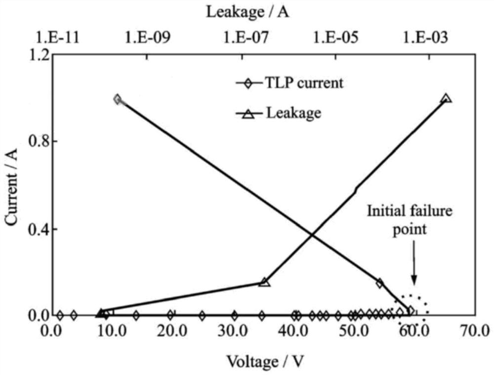
technical field [0001] The invention relates to the technical field of semiconductor integrated circuits, in particular to a novel silicon-controlled rectifier-type ESD protection structure without hysteresis effect and a realization method thereof. Background technique [0002] The anti-static protection design of high-voltage circuits has always been a technical problem, because the core of high-voltage circuits: high-voltage devices (such as LDMOS) are not suitable for anti-static protection design like ordinary low-voltage devices, because the hysteresis effect curve of high-voltage devices The exhibited characteristics are poor. Such as figure 1 as shown, figure 1 It is the hysteresis effect curve of a high-voltage device LDMOS with a working voltage of 32V, from figure 1 It can be concluded that: 1) the trigger voltage (Vt1) is too high; 2) the holding voltage (Vh) is too low, often far lower than the operating voltage of the high-voltage circuit, and it is easy to ...

Claims


Application Information

Patent Timeline
Patent Type & Authority Applications(China)
IPC IPC(8): H01L27/02H01L21/8228
CPCH01L27/0262H01L21/8228
Inventor 朱天志黄冠群陈昊瑜邵华
Owner SHANGHAI HUALI MICROELECTRONICS CORP
Learn More