Method for preparing N type battery by using insulating edge protective layer
A technology of insulating edge and protective layer, which is applied in the field of solar cells, can solve the problems affecting the overall efficiency of the cell, edge plating leakage, short circuit, etc., and achieve the effect of improving photoelectric efficiency, preventing the short circuit of the upper and lower electrodes of the silicon chip, and simple operation
- Summary
- Abstract
- Description
- Claims
- Application Information
AI Technical Summary
Problems solved by technology
Method used
Image
Examples
Embodiment 1
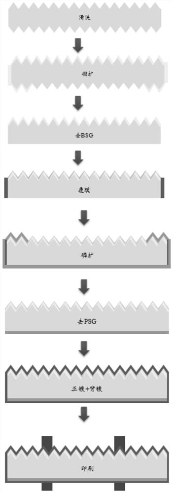
[0029] Wherein as preferably, the concrete operation condition of embodiment 1 efficient N-type TOPCon battery is:
[0030] (1) Cleaning and texturing treatment: select an N-type crystalline silicon substrate, remove metal ions on the N-type silicon wafer, and perform surface texturing and other treatments;
[0031] (2) Front boron diffusion: place the silicon wafer treated in step (1) in the furnace tube for boron diffusion, and the boron source used can be liquid BBr 3 Also gaseous BCl 3 , the diffusion temperature is 800~1200℃, and the diffusion time is 2h;
[0032] (3) Remove BSG: Put the silicon wafer after step (2) into the BSG removal equipment for back throwing and BSG removal treatment, wherein the solution used for back throwing is HCl / HNO 3 or NH 3 ﹒ h 2 O / H 2 o 2 Or one of the combinations of KOH / additive is used for back throwing, and 15% HF is used to remove the BSG layer on the surface.
[0033] (4) Apply the dielectric film evenly on the edge of the sil...
Embodiment 2
[0043] Embodiment 2 (wherein unrestricted condition is identical with embodiment 1)
[0044] (1) Select N-type monocrystalline silicon wafers, after cleaning, texturing, boron diffusion, and phosphorus washing;
[0045] (2) Apply the dielectric film evenly on the edge of the silicon wafer by using the roller transmission device;
[0046] The dielectric layer film is evenly applied to the edge of the silicon wafer by using a roller transmission device. The equipment used can uniformly apply the dielectric layer to a thickness of 3mm. The material of the dielectric layer is mainly glass powder and additives. The glass powder contains 90% by mass of glass powder and 10% by mass of ceramic powder, wherein: the glass powder is composed of the following components, calculated by mass percentage, 10% BaO, 25% ZnO, 30% B 2 o 3 , 30% SiO 2 , 3.5% Li 2 O and 1.5% Al 2 o 3 ; The ceramic powder is obtained by mixing alumina, zirconia, tin oxide and zinc oxide in equal mass ratios. ...
PUM
| Property | Measurement | Unit |
|---|---|---|
| thickness | aaaaa | aaaaa |
Abstract
Description
Claims
Application Information


