Preparation method of perovskite thin film and perovskite solar cell thereof
A solar cell and perovskite technology, applied in circuits, photovoltaic power generation, electrical components, etc., can solve the problems of fast attenuation, undurability, and impact on carrier transport performance, and achieve fewer defects, high crystal quality, and improved lubrication. wet effect effect
- Summary
- Abstract
- Description
- Claims
- Application Information
AI Technical Summary
Problems solved by technology
Method used
Image

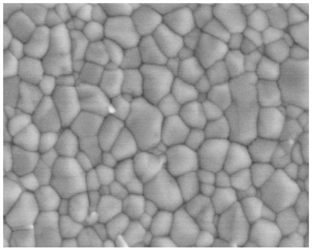
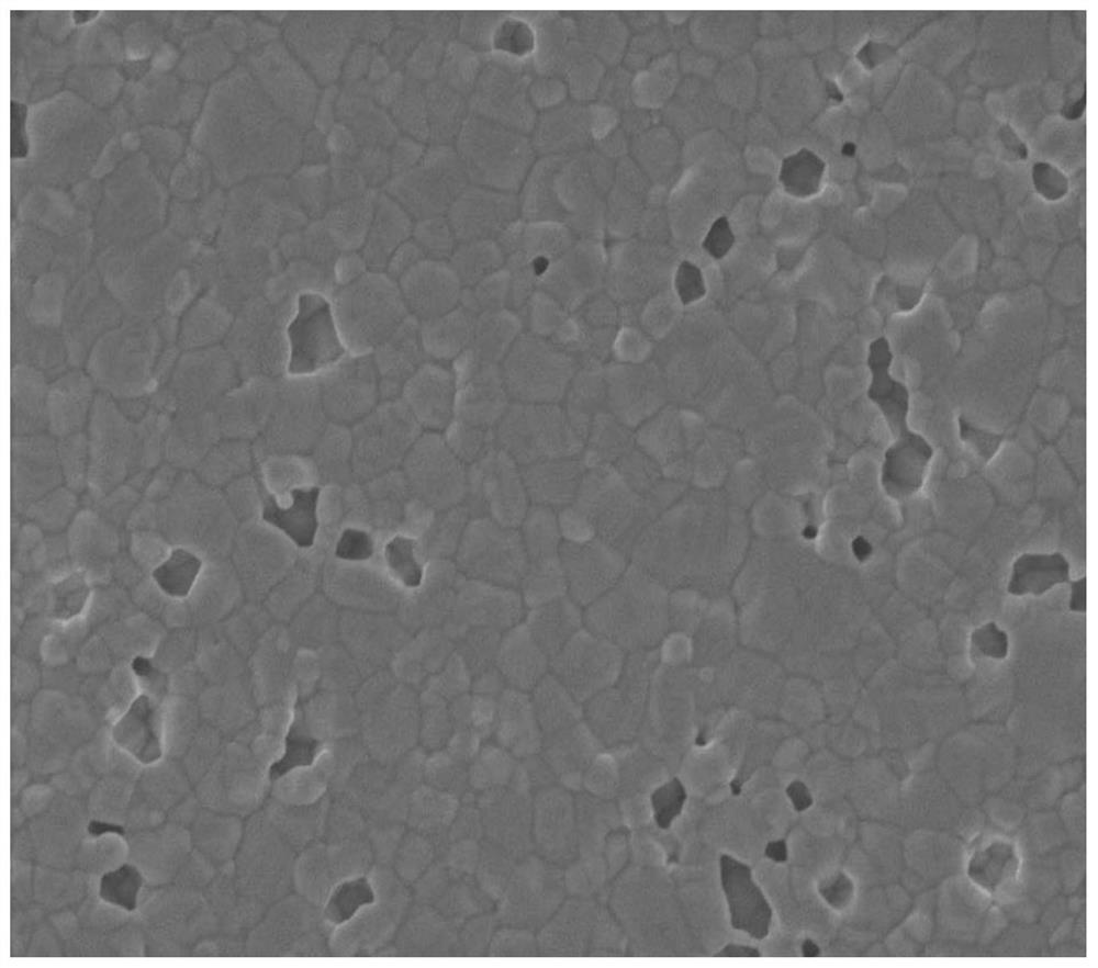
Examples
preparation example Construction
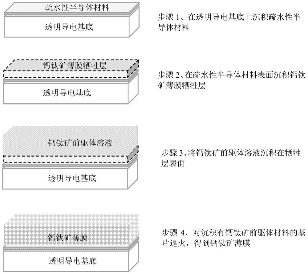
[0025] Please refer to figure 1 Shown, the preferred embodiment of the preparation method of perovskite film of the present invention, comprises the steps:
[0026] Step 1, depositing a hydrophobic semiconductor material on a transparent conductive substrate;
[0027] Step 2, depositing a perovskite film sacrificial layer on the surface of the hydrophobic semiconductor material;
[0028] Step 3, depositing the perovskite precursor solution on the surface of the sacrificial layer;
[0029] Step 4, annealing the substrate deposited with the perovskite precursor material to obtain a perovskite film.
[0030] Wherein, in step 1, the transparent conductive substrate has the characteristics of being highly transparent in the visible light and near-infrared light bands, and at the same time, has the ability to transport carriers, and has a light transmittance of not less than 80 in the wavelength range of 350nm to 800nm. %; the transparent conductive substrate includes a composite...
Embodiment 1
[0043] The preparation method embodiment 1 of perovskite film of the present invention comprises the following steps:
[0044] 11. Preparation of perovskite precursor solution: Dissolve 159g of methylamine hydriodide powder and 461g of lead iodide powder in 1 liter of mixed solvent of dimethyl sulfoxide and N,N-dimethylformamide, The resulting bright yellow solution was heated to 70 °C under magnetic stirring and kept for 2 h.
[0045] 12. Deposit a hydrophobic semiconductor film on a transparent conductive substrate: prepare 2 mg / ml PTAA chlorobenzene solution, spread evenly on the surface of ITO glass, spin-coat at 4000rpm / s for 20s, and anneal at 100°C for 10 minutes.
[0046] 13. Deposit the perovskite thin film sacrificial layer: place the substrate obtained in step 12 in the evaporation chamber, and the vacuum degree in the chamber is controlled at 10 -4 At about Pa, lead acetate was vapor-deposited on the surface of PTAA at an evaporation rate of 1 Å / s, and a 20-nanome...
Embodiment 2
[0050] The preparation method embodiment 2 of perovskite film of the present invention comprises the following steps:
[0051] 21. Preparation of perovskite precursor solution: Dissolve cesium iodide (CsI), formamidine hydriodide (FAI), lead iodide (PbI2), zinc bromide (Znbr2) powders in N-methylpyrrolidone In a mixed solvent with γ-butyrolactone, prepare 1.2 moles per liter of Cs0.05FA0.95PbI3(Znbr2)0.05 perovskite precursor solution, and heat the resulting bright yellow solution to 70°C under magnetic stirring conditions, And keep it for 2h.
[0052] 22. Depositing a hydrophobic semiconductor film on a transparent conductive substrate: select polyimide covered with aluminum-doped zinc oxide as the transparent conductive substrate, put it into the evaporation chamber, and control the vacuum degree in the chamber at 10 -4 At about Pa, while heating the substrate to 120°C, evaporate poly[[(4-butylphenyl)imino][1,1'-biphenyl]] at an evaporation rate of 0.5Å / s to obtain a thickn...
PUM
| Property | Measurement | Unit |
|---|---|---|
| Thickness | aaaaa | aaaaa |
| Thickness | aaaaa | aaaaa |
Abstract
Description
Claims
Application Information
 - R&D
- Intellectual Property
- Life Sciences
- Materials
- Tech Scout
- Unparalleled Data Quality
- Higher Quality Content
- 60% Fewer Hallucinations
Browse by: Latest US Patents, China's latest patents, Technical Efficacy Thesaurus, Application Domain, Technology Topic, Popular Technical Reports.
© 2025 PatSnap. All rights reserved.Legal|Privacy policy|Modern Slavery Act Transparency Statement|Sitemap|About US| Contact US: help@patsnap.com