
Patsnap Eureka
For R&D, Patsnap Eureka makes reading and utilizing patents & technical documents easy.
Patsnap Eureka AIR
Designed for self-driven R&D workflows. Generate viable solutions, solve complex R&D challenges, empower your innovation with AI.

Patsnap Eureka Materials
Designed for material experts only. Revolutionize your material R&D, from search, analyze, to developing new materials.

TechResearch
Generate reliable direction feasibility study reports for your R&D in just a few steps.

TechSeek
Discover and master advanced knowledge NOW. Basics, ideas, possibilities, all at once.

TechMind
As an expert in R&D Theories, TechMind can generates customized viable solutions instantly.

TechRisk
Analyze your overall solution with one click, know your potential R&D risks in advance.

TechMonitor
Get weekly tech updates, stay abreast of the latest tech innovations and key insights.
Copper-clad ceramic substrate and preparation method thereof
A technology of copper-clad ceramic substrate and ceramic layer, which is applied in the manufacture of semiconductor/solid-state devices, electrical components, electric solid-state devices, etc. The effect of thermal shock reliability improvement
- Summary
- Abstract
- Description
- Claims
- Application Information
AI Technical Summary
Problems solved by technology
Method used
Image

Examples
Embodiment 1
[0030] Embodiment 1 Copper-clad ceramic substrate
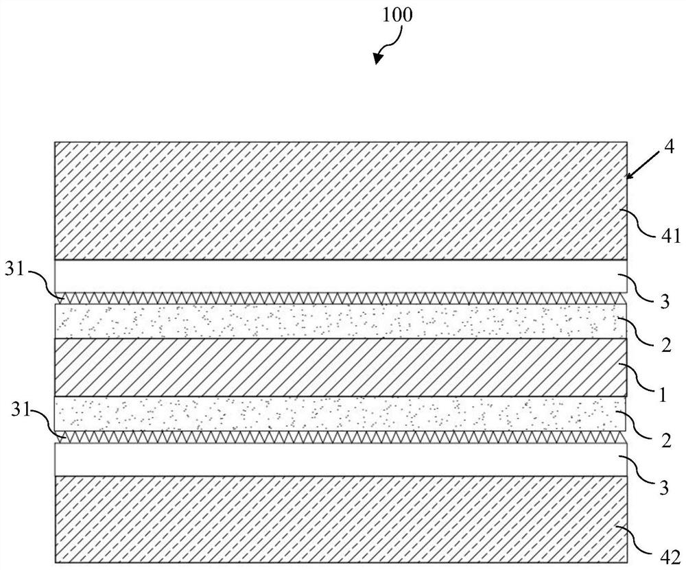
[0031] according to figure 1 , the structure of the copper-clad ceramic substrate 100 is as follows: before sintering, it includes a ceramic layer 1 located in the middle, a solder layer 2 located on the upper and lower sides of the ceramic layer, a stress buffer layer 3 attached to the solder layer, and a stress buffer layer attached to the stress buffer layer. Metal copper layer 4.
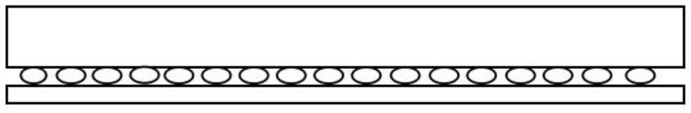
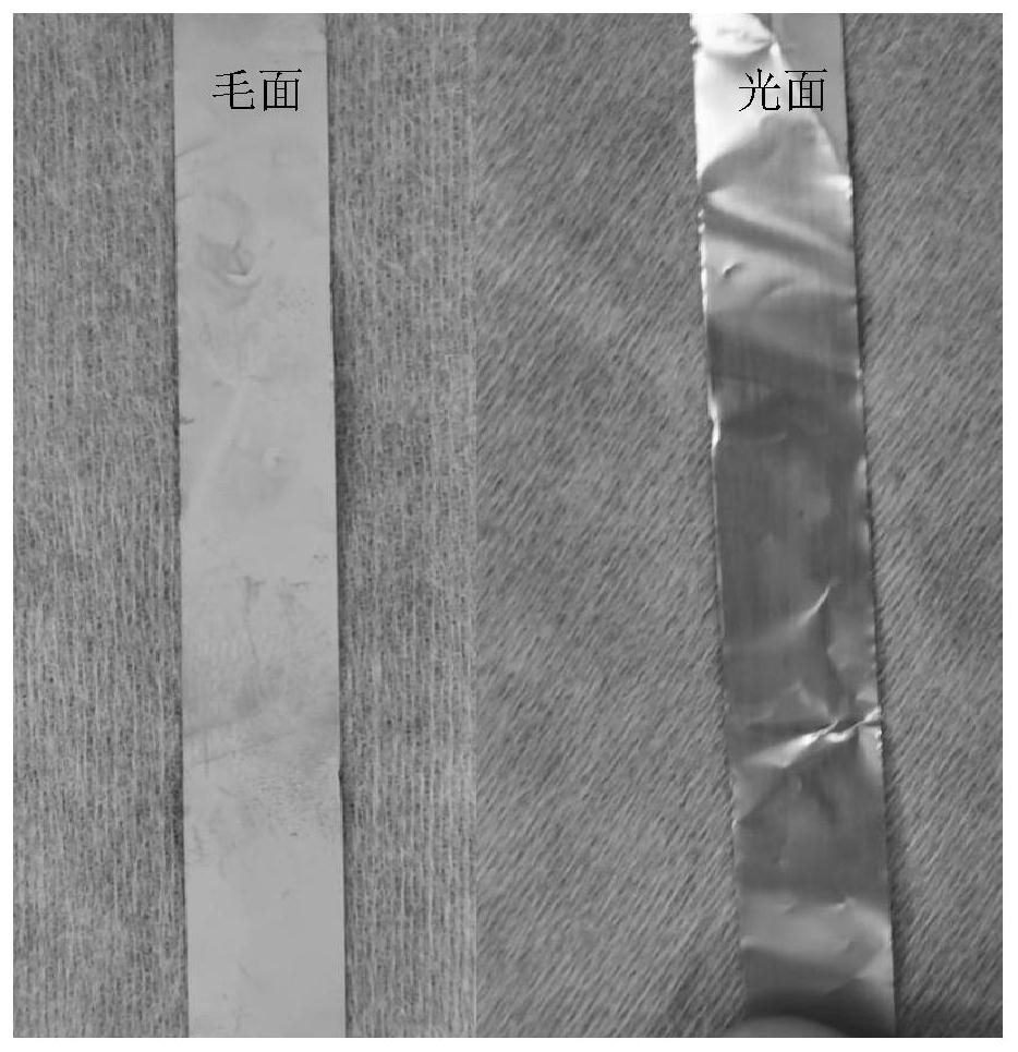
[0032] Wherein, the ceramic layer 1 is a silicon nitride ceramic plate or an aluminum nitride ceramic plate. The solder layer 2 includes two forms, one is solder arranged on both sides of the ceramic plate by screen printing, and the other is an active metal solder sheet attached to both sides of the ceramic plate. The stress buffer layer 3 is preferably copper foil, with the rough side 31 facing the solder layer and the smooth side facing the metal copper layer. After vacuum sintering, a microporous area ( figure 2 ).
[0033] In this em...
Embodiment 2
[0034] Embodiment 2 Copper-clad ceramic substrate preparation
[0035] 1) Use acetone or alcohol to degrease the copper foil as the stress buffer layer and the copper sheet as the metal copper layer, and then perform anti-oxidation cleaning;
[0036] 2) Double-sided screen-printed solder layer on the ceramic layer or double-sided pasting of active metal pads;
[0037] 3) Copper foil is pasted on the solder layer or the active metal solder sheet, and the copper foil is covered with a metal copper layer, the rough side of the copper foil faces the solder layer, and the smooth side faces the metal copper layer;
[0038] 4) Place indenters on the top and bottom of the parts to be sintered, such as glass, ceramics, graphite blocks or corundum bricks, etc.;
[0039] 5) Carry out vacuum active brazing sintering according to the AMB process and provide the required conditions for molecular diffusion welding. The temperature is controlled at 700°C-940°C, the vacuum degree is less than...
PUM
| Property | Measurement | Unit |
|---|---|---|
| thickness | aaaaa | aaaaa |
| thickness | aaaaa | aaaaa |
| thickness | aaaaa | aaaaa |
Abstract
Description
Claims
Application Information
 - R&D Engineer
- R&D Manager
- IP Professional
- Industry Leading Data Capabilities
- Powerful AI technology
- Patent DNA Extraction
Browse by: Latest US Patents, China's latest patents, Technical Efficacy Thesaurus, Application Domain, Technology Topic, Popular Technical Reports.
© 2024 PatSnap. All rights reserved.Legal|Privacy policy|Modern Slavery Act Transparency Statement|Sitemap|About US| Contact US: help@patsnap.com