IPD device based on DBC copper-clad plate and manufacturing process of IPD device
A technology of copper clad laminates and devices, which is applied in the direction of circuit substrate materials, electrical components, circuit thermal components, etc., can solve the problems of increasing process difficulty and time, increasing process complexity, increasing device insertion loss, etc.
- Summary
- Abstract
- Description
- Claims
- Application Information
AI Technical Summary
Problems solved by technology
Method used
Image

Examples
Embodiment 1
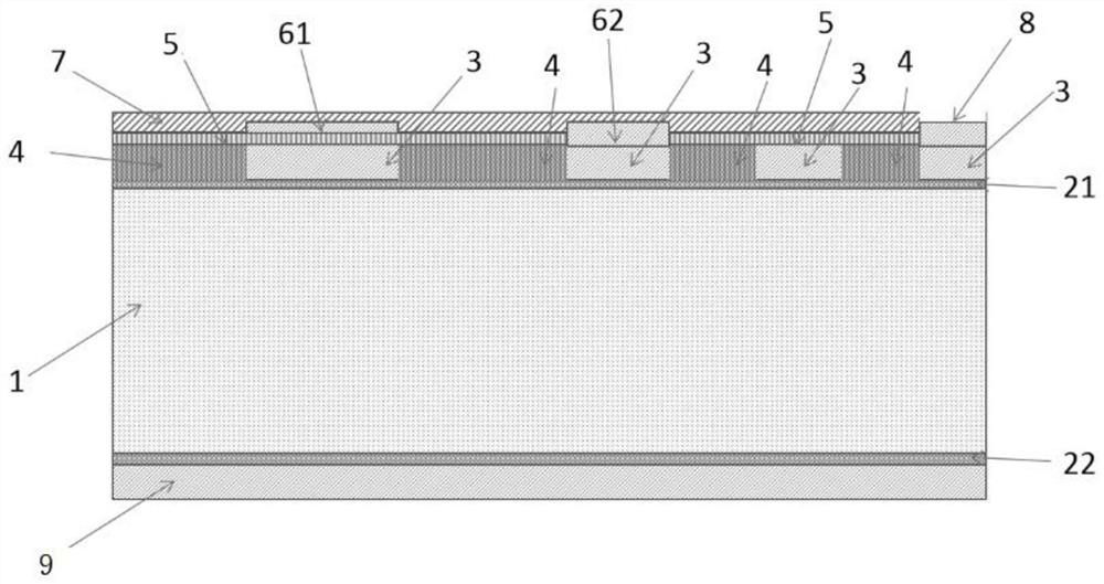
[0081] This embodiment shows an IPD device based on a DBC substrate, such as figure 1 As shown, including the substrate layer 1 and the through-substrate holes passing through it, the front and back sides of the substrate layer 1 each have a bonding layer, which are respectively the front bonding layer 21 and the back bonding layer 22, The back side of the back bonding layer 22 is covered with the back layer metal 9, and the front bonding layer 21 is sequentially formed with the bottom metal layer 3 and the upper layer metal layer 61, between the bottom metal layer 3 and the upper metal layer 61. A high dielectric constant dielectric layer 5 is deposited, and a passivation layer 7 is covered on the upper metal layer 61 .
[0082] Wherein, the substrate layer 1 is a ceramic layer with high thermal conductivity, such as aluminum nitride, zirconia, alumina and other ceramic glass materials with high thermal conductivity, high electrical insulation, high mechanical strength and lo...
Embodiment 2
[0091] This embodiment shows a high-pass filter manufactured by the IPD device process based on the DBC substrate, including the device circuit, structure, manufacturing process and use effect.
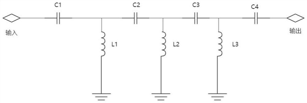
[0092] The equivalent circuit diagram of a high-pass filter is shown in figure 2As shown, the left and right ends are input and output ports, the signal enters the connection capacitor C1 from the left port, the other end of C1 is connected to the inductor L1 and C2, the other end of L1 is grounded, the other end of C2 is connected to the inductor L2 and capacitor C3, and the inductor L2 The other end of the capacitor C3 is connected to the ground, the other end of the capacitor C3 is connected to the inductor L3 and the capacitor C4, the other end of the inductor L3 is connected to the ground, the other end of the capacitor C4 is connected to the output port, and the signal is output from the right port. This circuit achieves the effect of high-pass filtering.
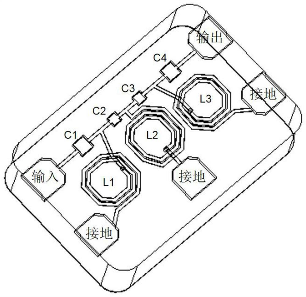
[0093] The top view...
Embodiment 3
[0120] This embodiment shows a bandpass filter manufactured by IPD device process based on DBC substrate, including device circuit, structure, manufacturing process and application effect.
[0121] The equivalent circuit diagram of the bandpass filter of the present embodiment is as Figure 5 As shown, the left and right ends are input and output ports, and the signal enters from the left port to connect capacitor C1 and inductor L1. Connect capacitor C3, and the other end of C3 is grounded. Inductor L3 is connected to the other end of capacitor C2, and connected to L4, inductor L5 and capacitor C4, the other end of inductor L4 is connected to capacitor C5, the other end of capacitor C5 is grounded, and the other end of inductor L5 is connected to capacitor C4, and connected to the output port. This circuit achieves the effect of bandpass filtering.
[0122] The top view structural diagram of the bandpass filter of this embodiment is as follows Figure 6 As shown, among them...
PUM
| Property | Measurement | Unit |
|---|---|---|
| Thickness | aaaaa | aaaaa |
| Thickness | aaaaa | aaaaa |
| Thickness | aaaaa | aaaaa |
Abstract
Description
Claims
Application Information
 - R&D
- Intellectual Property
- Life Sciences
- Materials
- Tech Scout
- Unparalleled Data Quality
- Higher Quality Content
- 60% Fewer Hallucinations
Browse by: Latest US Patents, China's latest patents, Technical Efficacy Thesaurus, Application Domain, Technology Topic, Popular Technical Reports.
© 2025 PatSnap. All rights reserved.Legal|Privacy policy|Modern Slavery Act Transparency Statement|Sitemap|About US| Contact US: help@patsnap.com