
Method for reducing optical band gap of indium sulfide semiconductor

A semiconductor and sulfide technology, which is applied in the field of reducing the optical band gap of In2S3 semiconductors, can solve problems such as inability to realize applications, and achieve the effects of reducing the band gap, expanding the scope of use, and increasing the absorption capacity.

Pending Publication Date: 2021-01-08
SHANGHAI DIANJI UNIV
View PDF3 Cites 0 Cited by
  • Summary
  • Abstract
  • Description
  • Claims
  • Application Information

AI Technical Summary

Problems solved by technology

However, the In obtained by this preparation method 2 S 3 Semiconductor thin films still cannot meet the requirement of a bandgap between 1.0eV and 1.5eV, so their application in semiconductor materials cannot be realized.

Method used


Image

  • Method for reducing optical band gap of indium sulfide semiconductor
  • Method for reducing optical band gap of indium sulfide semiconductor
  • Method for reducing optical band gap of indium sulfide semiconductor

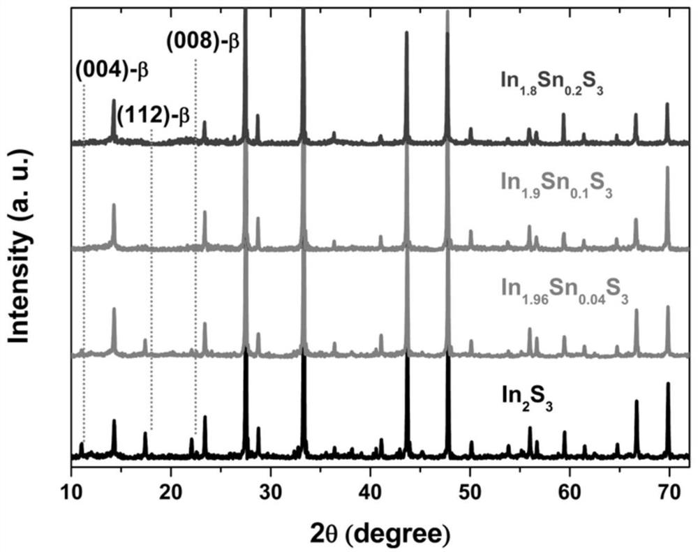
Examples


Embodiment

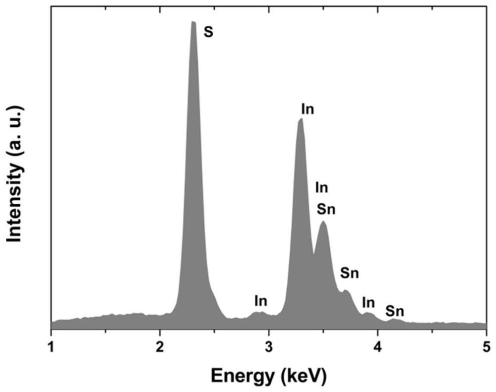
[0023] In 2-x sn x S 3 The samples are all sintered by vacuum solid state reaction. According to the stoichiometric ratio, In particles (5N), S powder (5N), and X (X=Sn) (4N) powder are vacuum-packed in a quartz tube, and the temperature is slowly raised to 850°C and kept for more than 24 hours. Finally, the sample is cooled in the furnace . The obtained sample was ground and repackaged, and re-sintered at 850°C for more than 24 hours to obtain the target powder sample for testing and characterization.

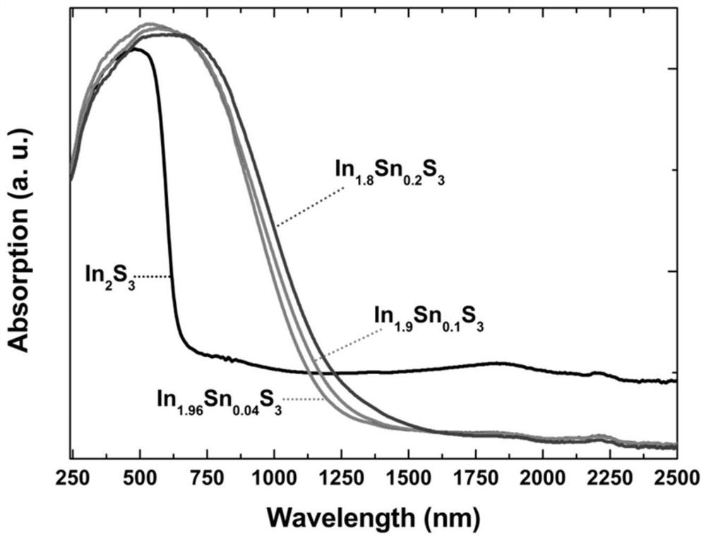
[0024] The X-ray diffraction pattern was measured on a Bruker D8 ADVANCE X-ray diffractometer. The UV-Vis-NIR absorption spectra of the materials were measured on a Hitachi U4100 UV-Vis-NIR spectrophotometer. The elemental analysis of materials was measured under a scanning electron microscope equipped with an energy dispersive spectrometer.

[0025] Based on the density functional theory framework, the electronic band structure in the case of Sn element doping was calcu...


PUM


Abstract

The invention relates to a method for reducing the optical band gap of an In2S3 semiconductor, and the method specifically comprises the steps: taking In2S3 binary sulfide as a parent semiconductor, regulating and controlling the energy band of the In2S3 binary sulfide through Sn element doping, and forming a semiconductor with the chemical formula of In2xSnxS3 (0.04<=x<=0.2). Compared with the prior art, the Sn element is doped in the In2S3 semiconductor, so that the forbidden band width of the In2S3 semiconductor material can be greatly reduced, and the absorption capacity of the In2S3 semiconductor material to a solar spectrum is improved, and therefore, the utilization range of the In2S3 semiconductor material is expanded, and the In2S3 semiconductor material can be directly used as asolar cell absorption material, and has practical significance for the development of solar cells.

Description

technical field [0001] The invention relates to the field of photovoltaic semiconductors, in particular to a method for reducing In 2 S 3 Semiconductor optical bandgap methods. Background technique [0002] Since the 21st century, with the rapid development of science and technology, the demand for energy is also increasing. The development of new energy utilization methods is the top priority of today's scientific development. Because solar energy has the advantages of abundant reserves, cleanness, local development and utilization, and no transportation problems, it has quickly become the focus of new energy development and utilization. The development of semiconductor solar cells has become an important way to utilize solar energy. Among them, the development of semiconductor absorber materials with excellent performance is the basis of solar cells. By adjusting the electronic band structure, optical properties and other photoelectric properties of semiconductor mater...

Claims


Application Information

Patent Timeline
IPC IPC(8): H01L31/0296H01L31/0216
CPCH01L31/02167H01L31/02168H01L31/02963Y02E10/50
Inventor 赵春燕张栋栋陈平
Owner SHANGHAI DIANJI UNIV
Learn More