Gate tube with superlattice-like structure and preparation method thereof

A technology similar to superlattice and gate tube, applied in the field of micro-nano electronics, can solve the problems of low threshold voltage, difficult to meet the requirements of high-performance gate tube, poor temperature and thermal stability, etc.

Active Publication Date: 2021-01-19
HUAZHONG UNIV OF SCI & TECH
View PDF5 Cites 1 Cited by
  • Summary
  • Abstract
  • Description
  • Claims
  • Application Information

AI Technical Summary

Problems solved by technology

Among them, the S atoms and Se atoms in GeS and GeSe have smaller radii and are more stable in bonding with Ge, so GeS and GeSe have good temperature and thermal stability, and are easy to form stable lattice orientations; but due to the GeS mobility band gap relatively wide, so its threshold voltage is relatively large
The atomic radius of Te in GeTe material is relatively large, therefore, the mobility band gap of GeTe is relatively small, so that it has a lower threshold voltage; but compared with GeS and GeSe, the temperature thermal stability is poor
Therefore, the comprehensive performance of the above materials is poor, and it is difficult to meet the requirements of high-performance gating tubes

Method used


Image

  • Gate tube with superlattice-like structure and preparation method thereof
  • Gate tube with superlattice-like structure and preparation method thereof

Examples


Embodiment Construction

[0026] In order to make the object, technical solution and advantages of the present invention clearer, the implementation manner of the present invention will be further described in detail below in conjunction with the accompanying drawings.

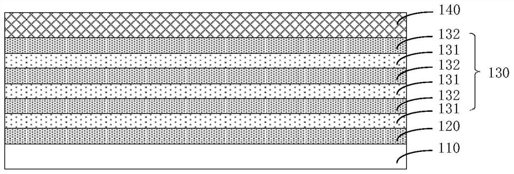
[0027] An embodiment of the present invention provides a gate transistor with a superlattice-like structure, figure 1 It is a structural schematic diagram of a gate tube with a superlattice-like structure provided by an embodiment of the present invention, as shown in figure 1 shown.

[0028] A gate tube with a superlattice-like structure, the gate tube includes a substrate 110, and a first metal electrode layer 120, a superlattice-like layer 130, and a second metal electrode layer 140 sequentially stacked on the substrate 110 , the superlattice-like layer 130 includes n+1 first sublayers 131 and n second sublayers 132 stacked alternately periodically, the material of the first sublayer 131 is GeS or GeSe, and the material of the seco...


PUM

PropertyMeasurementUnit
Thicknessaaaaaaaaaa
Thicknessaaaaaaaaaa

Abstract

The invention discloses a gating tube with a superlattice-like structure and a preparation method of the gating tube, and belongs to the technical field of micro-nano electronics. The gate tube comprises a substrate, and a first metal electrode layer, a superlattice-like layer and a second metal electrode layer which are sequentially stacked on the substrate; the superlattice-like layer comprisesn + 1 first sub-layers and n second sub-layers which are periodically and alternately stacked, the material of the first sub-layers comprises GeS or GeSe, and the material of the second sub-layers comprises one of GeTe, ZnTe, AlTe, SiTe, BTe or CTe. Due to the fact that the GeS material and the GeSe material have high stability, diffusion separation of Te in the second sub-layer material caused byhigh temperature can be prevented. Meanwhile, each sub-layer of the superlattice-like structure is very thin, the coupling between adjacent wells is very strong, periodic quantum potential wells areformed in the superlattice-like layer, and the original discrete energy levels in the quantum wells are expanded into energy bands, so the band gap width can be reduced, the power consumption is reduced, and the superlattice-like structure can be better integrated with a memory device unit.

Description

technical field [0001] The invention relates to the technical field of micro-nano electronics, in particular to a gate tube with a superlattice-like structure and a preparation method thereof. Background technique [0002] With the vigorous development of big data, cloud computing and Internet of Things industries, along with the explosive growth of massive information and the ever-expanding market demand, the efficient storage and convenient transmission of data are the strict requirements of contemporary storage technology. Performance storage technology also emerges as the times require. Among them, phase change memory technology has been widely recognized in the industry because of its relatively mature material system, simple preparation process, good compatibility with CMOS, high device reliability, and advantages in speed and service life. [0003] There is a problem of leakage current in the phase change memory, and the gate current may flow through the surrounding ...

Claims


Application Information

Patent Timeline
IPC IPC(8): H01L45/00
CPCH10N70/257H10N70/801H10N70/231H10N70/011
Inventor 童浩王伦王位国缪向水
Owner HUAZHONG UNIV OF SCI & TECH
Why Eureka
Try Eureka