Power module packaging structure and manufacturing method thereof

A technology of packaging structure and power module, which is used in semiconductor/solid-state device manufacturing, electrical components, electric solid-state devices, etc., can solve the problems of heat not being dissipated in time, over-temperature failure of power modules, etc., achieving a simple manufacturing process and eliminating heat. resistance and cost reduction

Pending Publication Date: 2021-01-29
湖南国芯半导体科技有限公司
View PDF9 Cites 0 Cited by
  • Summary
  • Abstract
  • Description
  • Claims
  • Application Information

AI Technical Summary

Problems solved by technology

However, the heat dissipation problem of the power module is closely related to its reliability, and the heat generated cannot be dissipated in time, which can easily cause the power module to overheat and fail.

Method used


Image

  • Power module packaging structure and manufacturing method thereof
  • Power module packaging structure and manufacturing method thereof
  • Power module packaging structure and manufacturing method thereof

Examples


Embodiment 1

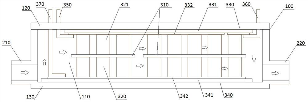
[0047] figure 1 It is a schematic structural diagram of the package structure of the power module in Embodiment 1 of the present application. Such as figure 1 As shown, in the assembled state, the upper electrode casing assembly of the package casing 100 of the power module packaging structure includes the upper casing 120 and the upper lining plate 330, and the lower electrode casing assembly includes the lower casing 130 and the lower lining plate 340, Wherein, the upper housing 120 is a plate structure, the lower housing 130 is a groove structure, the cooling liquid inlet 210 and the cooling liquid outlet 220 are both arranged on the lower housing 130, the upper housing 120 covers the opening of the lower housing 130 and Sealed tight connection is realized by screws.

[0048] Preferably, a sealing ring (not shown in the figure) is provided at the junction of the upper shell 120 and the lower shell 130 to further strengthen the sealing of the cavity 110 and prevent leakage...

Embodiment 2

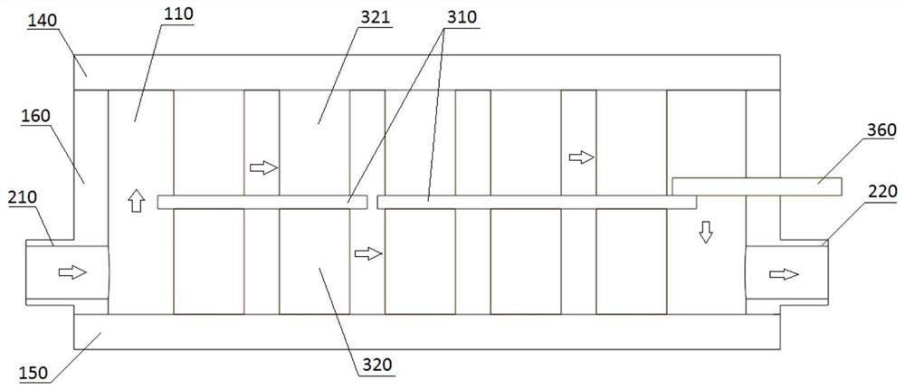
[0063] figure 2 It is a schematic diagram of a package structure of a power module provided in another embodiment of the present application. Such as figure 2As shown, the upper electrode casing assembly of the power module packaging structure includes an upper metal electrode 140, and the lower electrode casing assembly includes a lower metal electrode 150 and an intermediate casing 160, wherein the upper metal electrode 140 and the lower metal electrode 150 are both plate structure and can be directly connected to an external circuit, the coolant inlet 210 and the coolant outlet 220 are both arranged on the middle housing 160 , and the three are combined in a sealed manner to form the cavity 110 of the present application.

[0064] In this embodiment, the components of the power chip may also include a power chip 310 and upper surface metal pillars 321 and lower surface metal pillars 320 fixedly arranged on the upper surface of the power chip 310 .

[0065] When manufact...


PUM


Abstract

The invention provides a power module packaging structure and a manufacturing method thereof. The power module packaging structure comprises: at least one power chip; a packaging shell provided with acavity for accommodating a insulating cooling liquid and the power chip; and a cooling liquid inlet and a cooling liquid outlet which are formed in the packaging shell and are communicated with the cavity. The power chip is fixedly supported above the bottom wall of the cavity through a lower surface metal column located on the lower surface of the power chip, and the power chip is electrically connected with an external circuit through the lower surface metal column. By means of the packaging structure, the power chip can be directly and completely immersed in the insulating cooling liquid,heat can be dissipated on all surfaces of the power chip, heat dissipation paths are increased, and the heat dissipation problem of the high-density power module is solved.

Description

technical field [0001] The present invention relates to the field of power semiconductor packaging, and more specifically, to a power module packaging structure and a manufacturing method thereof. Background technique [0002] In order to meet the requirements of reducing energy consumption and extending the cruising range of electric vehicles, the power density of the insulated-gate bipolar transistor (Insulated-Gate Bipolar Transistor, “IGBT” for short) module of the electric drive system is getting higher and higher. IGBT module volume is reduced, power is increased, and more heat is generated in a smaller space, making heat dissipation of the power module a technical problem. In the traditional welding structure power module, the upper surface of the chip is covered by silica gel or epoxy resin with poor thermal conductivity. The heat generated by the chip can only be transmitted through the one-dimensional path of the lower surface of the chip, the liner, the substrate,...

Claims


Application Information

Patent Timeline
Patent Type & Authority Applications(China)
IPC IPC(8): H01L23/44H01L23/488H01L21/52H01L25/07H01L25/18H01L21/60
CPCH01L23/44H01L24/16H01L25/072H01L25/18H01L21/52H01L24/81H01L2224/16227
Inventor 姚亮齐放柯攀刘亮曾亮戴小平
Owner 湖南国芯半导体科技有限公司
Why Eureka
Try Eureka