Growth method of micro light-emitting diode epitaxial wafer

A technology of light-emitting diodes and a growth method is applied in the field of growth of micro-light-emitting diode epitaxial wafers, and can solve the problems of affecting the display effect of micro-LEDs, unevenness of epitaxial wafers, and increased warpage of epitaxial wafers.

Inactive Publication Date: 2021-02-02
HC SEMITEK SUZHOU
View PDF3 Cites 0 Cited by
  • Summary
  • Abstract
  • Description
  • Claims
  • Application Information

AI Technical Summary

Problems solved by technology

[0004] However, while Si provides electrons, it will also be doped in the epitaxial wafer as an impurity. The addition of Si changes the lattice growth of GaN itself, which will cause the stress in the N-type layer to increase.
And the higher the growth temperature of the N-type layer, the greater the stress in the N-type layer, which will cause the warping of the epitaxial wafer to increase, making the epitaxial wafer uneven
In the subsequent growth process of the active layer, the MO source (such as In source) cannot be evenly distributed on the epitaxial wafer, which will eventually lead to changes in the consistency of LED parameters (such as wavelength consistency, luminous intensity consistency, color consistency, etc.) Difference
For micro-LEDs with high consistency requirements, growing the N-type layer by the above method will seriously affect the display effect of micro-LEDs

Method used


Image

  • Growth method of micro light-emitting diode epitaxial wafer
  • Growth method of micro light-emitting diode epitaxial wafer
  • Growth method of micro light-emitting diode epitaxial wafer

Examples


Embodiment Construction

[0028] In order to make the purpose, technical solution and advantages of the present disclosure clearer, the implementation manners of the present disclosure will be further described in detail below in conjunction with the accompanying drawings.

[0029] figure 1 It is a flow chart of a method for growing a micro-LED epitaxial wafer provided by an embodiment of the present disclosure, as shown in figure 1 As shown, the growth method includes:

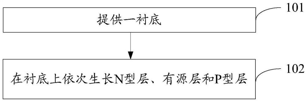
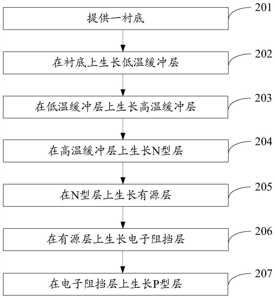
[0030] Step 101, providing a substrate.

[0031] Wherein, the substrate may be a sapphire substrate.

[0032] Step 102 , growing an N-type layer, an active layer and a P-type layer sequentially on the substrate.

[0033] Exemplarily, in step 102, growing an N-type layer on the substrate may include:

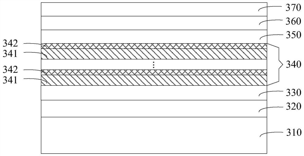
[0034] growing a first N-type layer and a second N-type layer alternately grown in multiple periods on the substrate;

[0035] Wherein, hydrogen and silane are introduced into the reaction chamber, and the first N-type layer is grow...


PUM

PropertyMeasurementUnit
temperatureaaaaaaaaaa
thicknessaaaaaaaaaa
thicknessaaaaaaaaaa

Abstract

The invention provides a growth method of a micro light emitting diode epitaxial wafer, which belongs to the technical field of semiconductors. The growth method comprises the following steps of providing a substrate, and sequentially growing an N-type layer, an active layer and a P-type layer on the substrate. The step of growing the N-type layer on the substrate comprises the sub-steps of growing a plurality of first N-type layers and second N-type layers on the substrate, wherein the first N-type layers and the second N-type layers grow periodically and alternately, introducing hydrogen andsilane into the reaction chamber, growing a first N-type layer under the high-temperature condition, wherein the first N-type layer is a Si-doped GaN layer, and stopping introducing hydrogen and silane into the reaction chamber, reducing the temperature in the reaction chamber, and growing a second N-type layer on the first N-type layer, wherein the second N-type layer is an undoped GaN layer. Byadopting the growth method, the stress in the N-type layer can be repeatedly released for multiple times, the warping of the epitaxial wafer is greatly improved, the consistency of various parametersof the micro light emitting diode is better, and the requirement of high consistency of various parameters of the micro light emitting diode is met.

Description

technical field [0001] The present disclosure relates to the technical field of semiconductors, in particular to a method for growing micro-LED epitaxial wafers. Background technique [0002] A light-emitting diode (English: Light Emitting Diode, referred to as: LED) is a semiconductor electronic component that can emit light. As a new type of high-efficiency, environmentally friendly and green solid-state lighting source, LED is being rapidly and widely used in fields such as traffic lights, automotive interior and exterior lights, urban landscape lighting, indoor and outdoor display screens, and small-pitch display screens. [0003] The epitaxial wafer is the primary product in the LED manufacturing process. In related technologies, an LED epitaxial wafer includes a substrate and an N-type layer, an active layer and a P-type layer stacked on the substrate in sequence. Wherein, the N-type layer is a GaN layer heavily doped with Si, which is used to provide electrons, elec...

Claims


Application Information

Patent Timeline
Patent Type & Authority Applications(China)
IPC IPC(8): H01L33/00H01L33/02H01L33/12C23C16/455C23C16/30
CPCC23C16/303C23C16/45523H01L33/005H01L33/007H01L33/025H01L33/12
Inventor 姚振从颖董彬忠李鹏
Owner HC SEMITEK SUZHOU
Why Eureka
Try Eureka