A method for preparing submicron concentric rings on silicon surface by femtosecond laser

A femtosecond laser, concentric ring technology, applied in the field of laser applications, to achieve the effect of low cost and simple process

Active Publication Date: 2021-08-24
BEIJING INSTITUTE OF TECHNOLOGYGY
View PDF15 Cites 0 Cited by
  • Summary
  • Abstract
  • Description
  • Claims
  • Application Information

AI Technical Summary

Problems solved by technology

However, the period of the concentric ring structures prepared by the above method is between a few microns and more than ten microns, so that they are not in the order of submicron and nanometer

Method used


Image

  • A method for preparing submicron concentric rings on silicon surface by femtosecond laser
  • A method for preparing submicron concentric rings on silicon surface by femtosecond laser
  • A method for preparing submicron concentric rings on silicon surface by femtosecond laser

Examples


Embodiment 1

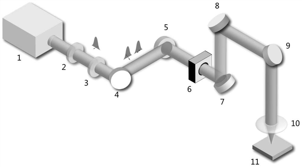
[0022] A method for preparing submicron concentric rings on a silicon surface with a femtosecond laser, the specific steps are as follows:

[0023] Step (1) Use femtosecond laser 1 to generate 800nm ​​horizontally polarized femtosecond laser single pulse, and adjust the focused laser energy density to about twice (1.6 times to 2.2 times range), about 1.0J / cm 2 ;

[0024] Step (2) is that the yttrium vanadate crystal 3 of 1.2mm is penetrated by the femtosecond laser single pulse perpendicular incidence in the step (1), and the yttrium vanadate crystal 3 is rotated so that its optical axis is in line with that of the step (1). The angle between the polarization direction of the femtosecond laser single pulse is 45°, and the femtosecond laser double pulse sequence with the polarization directions perpendicular to each other, the pulse energy equal, and the pulse delay about 0.85ps is obtained;

[0025] Step (3) Modify the repetition frequency of the femtosecond laser 1 to 10 Hz...

Embodiment 2

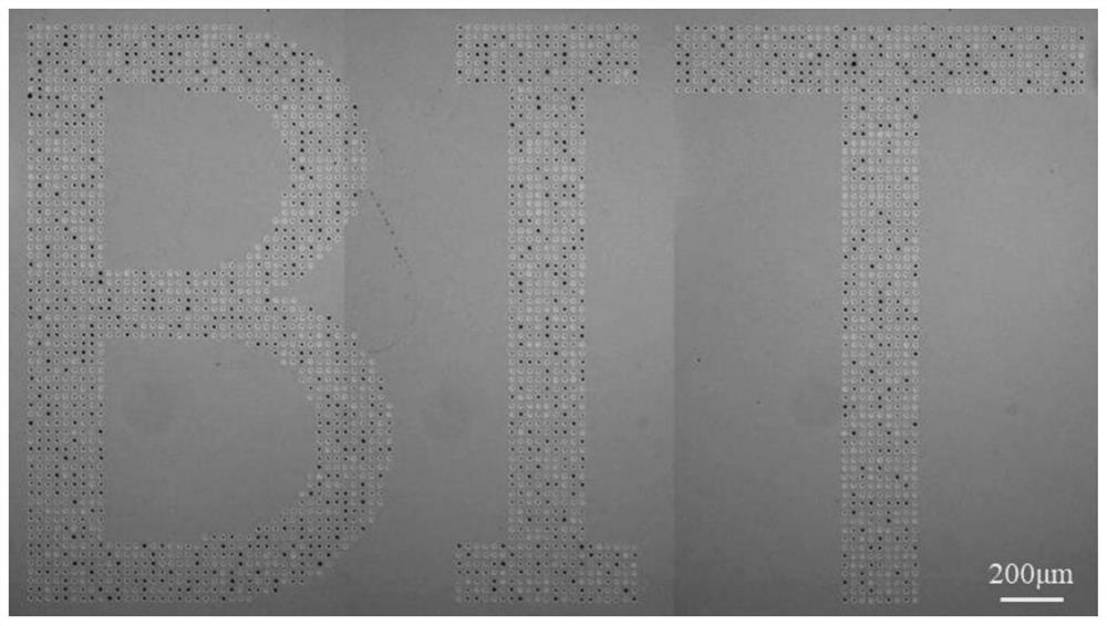
[0030] By adopting the method of the present invention, a large-area submicron concentric ring array is prepared on the silicon surface, and applied to the display of structural color.

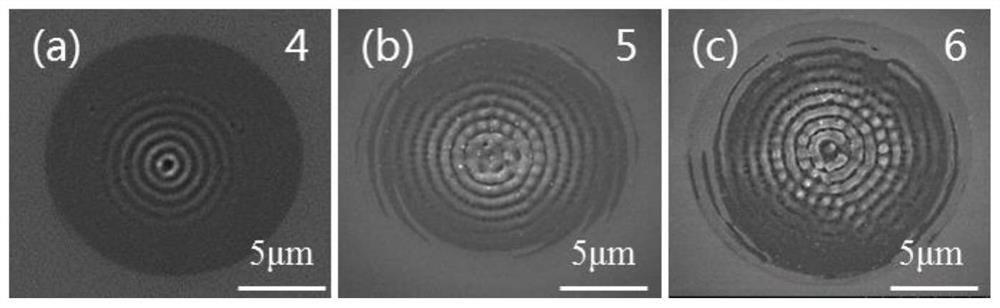
[0031] The processing equipment and femtosecond laser processing parameters are the same as in Example 1. A large-area submicron concentric ring array in the shape of "BIT" is processed on the surface of the silicon wafer, and the area size is 3.7mm*2mm. Such as image 3 Shown is an optical microscope image of the processed area. Since the concentric ring structure has diffraction gratings in all directions, when white light is used to irradiate the processing area vertically, such as Figure 4 In the method shown, the structural color can be observed in all directions by rotating the sample where the processing area is located. The advantage of the present invention is that, compared with the traditional parallel linear grating structure, the structural color can only be observed in one di...


PUM


Abstract

The invention relates to a method for preparing submicron concentric rings on a silicon surface with a femtosecond laser, belonging to the field of laser applications. In the present invention, a femtosecond laser single pulse is vertically incident through a yttrium vanadate crystal with a certain thickness to obtain a femtosecond laser double pulse sequence with a certain pulse delay whose polarization directions are perpendicular to each other and pulse energy is equal. The thickness of the yttrium vanadate crystal is The range of the femtosecond laser pulse should be satisfied, so that the delay range of the double pulse pulse generated after the femtosecond laser single pulse of the corresponding wavelength is about 0.5ps‑1.5ps; then use the attenuation sheet to adjust the total energy density of the femtosecond laser double pulse to the sample to be processed 1.6 to 2.2 times the ablation threshold of the material silicon; then this vertically polarized femtosecond laser double pulse is vertically focused on the surface of the material to be processed through a plano-convex lens; the number of pulse sequences focused on the surface of the material is controlled by the opening time of the optical switch For 4‑6 pieces, a single point of irradiation on the surface of the silicon material can prepare a submicron concentric ring structure on the silicon surface.

Description

technical field [0001] The invention relates to a method for preparing submicron concentric rings on a silicon surface with a femtosecond laser, belonging to the field of laser applications. Background technique [0002] Currently, the fabrication of submicron and nanoscale concentric ring structures has attracted a great deal of research interest due to the great potential of such structures in the fields of plasmonic lens fabrication, surface-enhanced Raman scattering, laser beam shaping, and modulation of photonic nanojets. research value. Currently, methods such as electron beam lithography, focused ion beam lithography, and template-assisted methods can be used to fabricate nanoconcentric structures with high quality. However, these methods require expensive devices as well as complex fabrication processes and vacuum environments, making their preparation costly. [0003] In the document "Appl Surf Sci 2010; 256:3653-3660.", a linearly polarized laser was used to proc...

Claims


Application Information

Patent Timeline
Patent Type & Authority Patents(China)
IPC IPC(8): B23K26/36B23K26/064B23K26/0622
CPCB23K26/0643B23K26/0648B23K26/36B23K26/0622B23K26/064B23K2103/56
Inventor 姜澜刘威胡洁邱兆岭
Owner BEIJING INSTITUTE OF TECHNOLOGYGY
Why Eureka
Try Eureka