Metal base substrate
A metal base, metal substrate technology, applied in metal pattern materials, circuit substrate materials, metal layered products, etc., can solve the problems of high thermal expansion rate, reduced insulation layer elasticity, low thermal expansion rate, etc., and achieve the effect of suppressing solder cracks
- Summary
- Abstract
- Description
- Claims
- Application Information
AI Technical Summary
Problems solved by technology
Method used
Image
Examples
Embodiment
[0065] Hereinafter, the effects of the present invention will be described through examples.
[0066] [Example 1 of the present invention]
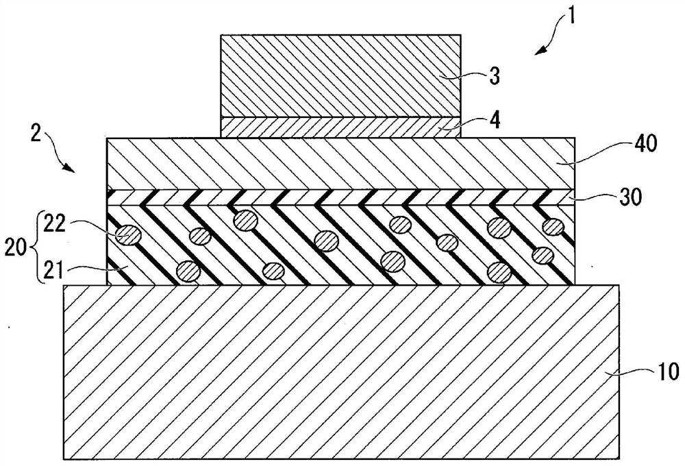
[0067]4,4'-Diaminodiphenyl ether and NMP (N-methyl-2-pyrrolidine) were placed in a 300 mL separable flask. The amount of NMP was adjusted so that the density|concentration of the obtained polyamic acid might become 40 mass %. After stirring at room temperature to completely dissolve 4,4'-diaminodiphenyl ether, a predetermined amount of tetracarboxylic dianhydride was added little by little so that the internal temperature did not exceed 30°C. Then, stirring was continued for 16 hours under a nitrogen atmosphere to prepare a polyamic acid (polyimide precursor) solution.
[0068] Alumina particles (average particle diameter: 0.5 μm) were prepared as ceramic particles (thermally conductive filler). The prepared 1.0 g of alumina particles and 10 g of NMP were mixed and subjected to ultrasonic treatment for 30 minutes to prepare an alumina ...
example 4
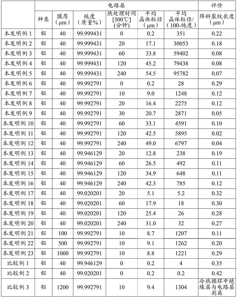
[0087] Except that the film thickness, purity, average crystal grain size and average crystal grain size / (100-purity) are the values shown in Table 2 below instead of aluminum foil, metal The base substrate, and the crack length of the solder layer after applying a thermal cycle was measured. The average crystal grain size and the average crystal grain size / (100-purity) of the copper foil were adjusted by performing heat treatment at a temperature of 300° C. for a heat treatment time shown in Table 2 below. In addition, regarding the purity of the copper foil, except that the impurity elements are Na, Mg, Si, Al, P, K, Ca, Ti, V, Cr, Mn, Fe, Co, Ni, Zn, Ga, Ge, Nb, Mo, Ru, Pd, Ag, In, Sn, Sb, Ba, Hf, W, Pt, Au, Pb, and Bi were measured in the same manner as the purity of aluminum foil. About the average crystal grain diameter of copper foil, it measured similarly to the average crystal grain diameter of aluminum foil.
[0088] [Table 2]
[0089]
[0090] Regarding the ...
PUM
| Property | Measurement | Unit |
|---|---|---|
| thickness | aaaaa | aaaaa |
| crystal size | aaaaa | aaaaa |
| crystal size | aaaaa | aaaaa |
Abstract
Description
Claims
Application Information


