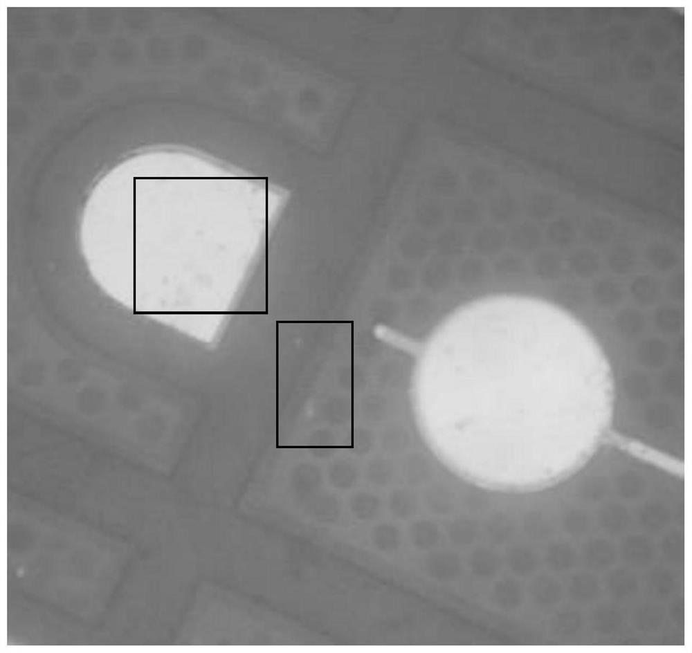
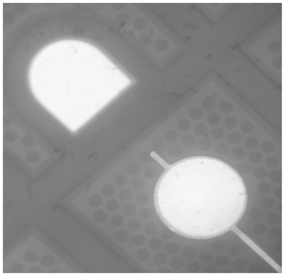
Semiconductor chip bonding wax cleaning agent as well as preparation method and use method thereof
A semiconductor and cleaning agent technology, which is applied in the manufacture of semiconductor/solid-state devices, the preparation of detergent mixture compositions, chemical instruments and methods, etc., can solve the problems of incomplete cleaning of bonding wax, complex process, and large safety hazards. Achieve the effect of improving cleaning efficiency and thoroughness, simple process, and preventing sticking back
- Summary
- Abstract
- Description
- Claims
- Application Information
AI Technical Summary
Problems solved by technology
Method used
Image
Examples
Embodiment 1
[0038] A kind of semiconductor chip bonding wax cleaning agent, raw material is as shown in table 1:
[0039] Table 1 A semiconductor chip bonding wax cleaning agent component table
[0040]
[0041] The preparation method step of semiconductor chip bonding wax cleaning agent is as follows:
[0042] (1) The cleaning agent is produced in a thousand-level ultra-clean production workshop (open the air purification system, the particle size content is less than 1000 per cubic foot, and the dust particles of 0.5um are less than 1000), and the materials used are above 95%. The ambient temperature is 24-26°C, and the humidity is 40%-60%.
[0043] (2) After the reaction kettle used in production is fully rinsed with pure water and air-dried, the reactor is rinsed twice with ethylene glycol tert-butyl ether, and air-dried for later use (completed before production).
[0044] (3) Add alcohol ether solvent (ethylene glycol tert-butyl ether) in the reaction kettle, then add the abiet...
Embodiment 2
[0049] A kind of semiconductor chip bonding wax cleaning agent, raw material is as shown in table 2:
[0050] Table 2 A semiconductor chip bonding wax cleaning agent component list
[0051]
[0052]
[0053] The preparation method step of semiconductor chip bonding wax cleaning agent is as follows:
[0054] (1) The cleaning agent is produced in a thousand-level ultra-clean production workshop (open the air purification system, the particle size content is less than 1,000 dust particles of 0.5um per cubic foot), and the materials used are above 98%. The ambient temperature is 24-26°C, and the humidity is 40%-60%.
[0055] (2) After the reaction kettle used in production is fully rinsed with pure water and air-dried, the reactor is rinsed with tripropylene glycol methyl ether twice, and air-dried for later use (completed before production).
[0056] (3) Tripropylene glycol methyl ether is added in the reactor, and then the cleaning synergist (Span and Tween composition) of...
Embodiment 3
[0061] A kind of semiconductor chip bonding wax cleaning agent, raw material is as shown in table 3:
[0062] Table 3 A semiconductor chip bonding wax cleaning agent component table
[0063]
[0064] The preparation method step of semiconductor chip bonding wax cleaning agent is as follows:
[0065] (1) The cleaning agent is produced in a thousand-level ultra-clean production workshop (open the air purification system, the particle size content is less than 1000 per cubic foot, and the dust particles of 0.5um are less than 1000), and the materials used are above 90%. The ambient temperature is 24-26°C, and the humidity is 40%-60%.
[0066] (2) After the reaction kettle used in production is fully rinsed with pure water and air-dried, the reactor is rinsed twice with ethylene glycol tert-butyl ether, and air-dried for later use (completed before production).
[0067] (3) In the reactor, first add the calculated amount of tripropylene glycol methyl ether, then add the calcu...
PUM
 Abstract
Description
Claims
Application Information
 - R&D
- Intellectual Property
- Life Sciences
- Materials
- Tech Scout
- Unparalleled Data Quality
- Higher Quality Content
- 60% Fewer Hallucinations
Browse by: Latest US Patents, China's latest patents, Technical Efficacy Thesaurus, Application Domain, Technology Topic, Popular Technical Reports.
© 2025 PatSnap. All rights reserved.Legal|Privacy policy|Modern Slavery Act Transparency Statement|Sitemap|About US| Contact US: help@patsnap.com


