Chip-level packaging structure for moisture sensitive high color gamut backlight application and manufacturing method

A chip-level packaging and manufacturing method technology, applied in the field of backlight, can solve the problems of poor operating performance of the sorting machine, easy scratches on the surface of the package, poor thermal conductivity of silica gel, etc., and achieve easy sorting machine operation and excellent heat resistance Performance, the effect of avoiding scratches

Active Publication Date: 2021-03-26
TECORE SYNCHEM
View PDF6 Cites 0 Cited by
  • Summary
  • Abstract
  • Description
  • Claims
  • Application Information

AI Technical Summary

Problems solved by technology

[0003] Backlight applications usually use medium and high-power LED CSPs. When the blue light emitted by the chips excites phosphors, a large amount of heat is released, and the thermal conductivity of silica gel is poor. The problem of glue cracking leads to failure or changes in color coordinates, so it is necessary to solve the heat dissipation problem of the package
The hardness of silica gel is relatively low, the surface of the package is easy to scratch, and the performance of the sorting machine is not good, so it is necessary to increase the hardness of the package

Method used


Image

  • Chip-level packaging structure for moisture sensitive high color gamut backlight application and manufacturing method
  • Chip-level packaging structure for moisture sensitive high color gamut backlight application and manufacturing method
  • Chip-level packaging structure for moisture sensitive high color gamut backlight application and manufacturing method

Examples


Embodiment Construction

[0037]The technical solutions of the present invention will be further described below in conjunction with specific embodiments. Those skilled in the art can easily understand the advantages of the present invention through the content in the specification. Before further describing the specific embodiments of the present invention, it should be understood that the scope of protection of the present invention is not limited to the following specific examples; the experimental methods that do not indicate specific conditions in the following examples are usually according to conventional conditions, or according to conditions recommended by the manufacturer. When the examples give numerical ranges, it should be understood that, unless otherwise stated in the present invention, the two endpoints of each numerical range and any value between the two endpoints can be selected.

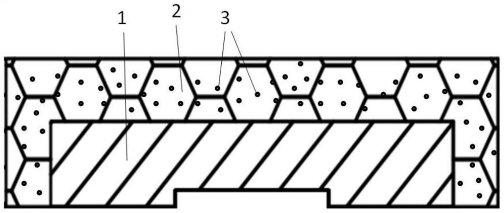
[0038] figure 1 It is a structural schematic diagram of a common five-sided light-emitting CSP in the...


PUM

PropertyMeasurementUnit
Thicknessaaaaaaaaaa
Thicknessaaaaaaaaaa
Viscosityaaaaaaaaaa

Abstract

The invention discloses a chip-level packaging structure for moisture-sensitive high-color-gamut backlight application. The chip-level packaging structure is of a double-layer packaging structure, wherein the inner layer is a fluorescent glue film containing KSF fluorescent powder; and the outer layer is a transparent adhesive film containing an inorganic filler. Firstly, an LED chip array is inversely arranged on a substrate, secondly, five surfaces of a chip are attached to a fluorescent adhesive film containing KSF fluorescent powder in a vacuum shape-preserving mode, then, a bottom adhesive film is cut along the outer vertical surface of a packaging body, then, the cut packaging body is arranged on the substrate in a secondary array mode, an organic silicon transparent adhesive film containing micron-sized inorganic filler is packaged outside the cut packaging body through vacuum pressing, and finally, the CSP packaging body is cut after curing. The CSP packaging body has excellentmoisture resistance and high hardness, heat conduction and light attenuation resistance, can be used for high-power LED devices, and improves the overall performance of the finished CSP packaging body.

Description

technical field [0001] The invention relates to the field of backlights, in particular to a chip-level packaging structure and a manufacturing method for moisture-sensitive high-color-gamut backlight applications. Background technique [0002] With the maturity of flip-chip LED chip CSP (Chip Scale Package) manufacturing technology, TFT-LCD (Thin Film Transistor Liquid Crystal Display) using CSP (Chip Scale Package) white LEDs as backlight components has gradually become the mainstream. In order to pursue high color gamut To display the effect, the LED phosphor uses a combination of KSF fluoride phosphor and β-SiAlON phosphor with a narrow half-peak width. KSF phosphors will deteriorate due to chemical reactions when exposed to water. Although phosphor manufacturers have carried out phosphor surface passivation treatment, for long-term reliability requirements, simple surface treatment of KSF phosphors cannot prevent the entry of water vapor, that is, The purpose of protect...

Claims


Application Information

Patent Timeline
IPC IPC(8): H01L33/54H01L33/50H01L33/56
CPCH01L33/54H01L33/56H01L33/502H01L2933/0033H01L2933/005H01L33/50B29C37/00B29C48/08C08K3/013C09J7/22C09J11/04C09J9/00C09J183/04C09K11/00H01L23/00H01L23/31H01L23/564H01L23/3135B29C37/0075C09J2301/312C09J2301/208
Inventor 韩颖谭晓华刘东顺冯亚凯
Owner TECORE SYNCHEM
Why Eureka
Try Eureka