Micro-nano single crystal flexible photoelectric detector with groove array structure and preparation method thereof

A photodetector and array structure technology, which is applied in photovoltaic power generation, electric solid-state devices, organic semiconductor devices, etc., can solve the problem of less research on micro-nano structure regulation of photodetector devices, and achieve the effect of enhancing photoelectric detection performance and low cost.

Active Publication Date: 2021-04-06
TONGJI UNIV
View PDF15 Cites 5 Cited by
  • Summary
  • Abstract
  • Description
  • Claims
  • Application Information

AI Technical Summary

Problems solved by technology

[0005] However, the controllable preparation of perovskite micro-nano single crystals and the application of flexible devices are still in the nascent stage, and further development still faces many challenges, such as crystal quality and The performance needs to be further improved, the complex patterning process with nanometer resolution has yet to be explored, and the application of functionalized devices, etc.
At the same time, there are few studies on the regulation of the micro-nano structure of photodetector devices.

Method used


Image

  • Micro-nano single crystal flexible photoelectric detector with groove array structure and preparation method thereof
  • Micro-nano single crystal flexible photoelectric detector with groove array structure and preparation method thereof

Examples


Embodiment 1

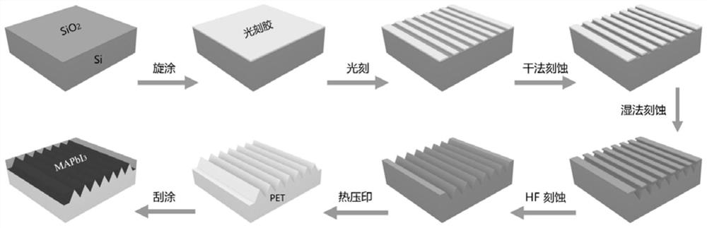
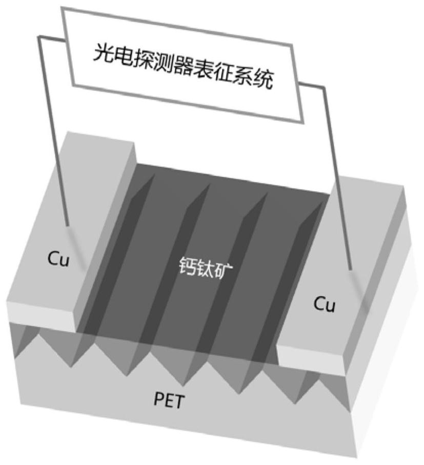
[0037] The preparation process of perovskite micro-nano single crystal flexible photodetector with enhanced photoelectric performance with trench array structure is as follows: figure 1 As shown, it specifically includes the following steps:

[0038] 1) Preparation of groove array micro-nano structure silicon template

[0039] 1-1) Clean the silicon wafer whose surface is covered with silicon dioxide with a thickness of 300 nanometers:

[0040] Ultrasonic cleaning with concentrated sulfuric acid for 20-30 minutes;

[0041] Ultrasonic cleaning with deionized water for 20-30 minutes;

[0042] Ultrasonic cleaning with ethanol for 20-30 minutes;

[0043] Ultrasonic cleaning with acetone for 20-30 minutes;

[0044] Wash with isopropanol for 20-30 minutes.

[0045] 1-2) Oxygen plasma etching

[0046] The cleaned silicon substrate needs to be dried with a nitrogen flow, and then placed in a dry etcher, and etched with oxygen plasma for 3-5 minutes, so as to improve the surface ...

Embodiment 2

[0068] A method for preparing a micro-nano single crystal flexible photodetector with a trench array structure, the method comprising the following steps:

[0069] 1) Prepare a silicon template with groove array micro-nano structure:

[0070] 1-1) cleaning the silicon wafer with a silicon dioxide layer on the surface;

[0071] 1-2) performing oxygen plasma etching on the cleaned silicon wafer;

[0072] 1-3) spin coating photoresist on the silicon dioxide layer of silicon wafer;

[0073] 1-4) performing deep ultraviolet lithography on the photoresist on the silicon dioxide layer;

[0074] 1-5) developing the silicon wafer after photolithography, and cleaning off the unexposed photoresist;

[0075] 1-6) dry etching the silicon dioxide layer on the silicon wafer;

[0076] 1-7) wet etching the silicon wafer after dry etching;

[0077] 1-8) Remove the remaining SiO on the surface of the silicon wafer 2 , to obtain a silicon template with a groove array micro-nano structure; ...

Embodiment 3

[0093] A method for preparing a micro-nano single crystal flexible photodetector with a trench array structure, the method comprising the following steps:

[0094] 1) Prepare a silicon template with groove array micro-nano structure:

[0095] 1-1) cleaning the silicon wafer with a silicon dioxide layer on the surface;

[0096] 1-2) performing oxygen plasma etching on the cleaned silicon wafer;

[0097] 1-3) spin coating photoresist on the silicon dioxide layer of silicon wafer;

[0098] 1-4) performing deep ultraviolet lithography on the photoresist on the silicon dioxide layer;

[0099] 1-5) developing the silicon wafer after photolithography, and cleaning off the unexposed photoresist;

[0100] 1-6) dry etching the silicon dioxide layer on the silicon wafer;

[0101] 1-7) wet etching the silicon wafer after dry etching;

[0102] 1-8) Remove the remaining SiO on the surface of the silicon wafer 2 , to obtain a silicon template with a groove array micro-nano structure; ...


PUM

PropertyMeasurementUnit
thicknessaaaaaaaaaa
thicknessaaaaaaaaaa
thicknessaaaaaaaaaa

Abstract

The invention relates to a micro-nano single crystal flexible photoelectric detector with a groove array structure and a preparation method thereof. The preparation method comprises the following steps: 1) preparing a silicon template with the groove array micro-nano structure; 2) transferring the groove array micro-nano structure on the silicon template to a flexible substrate by adopting a hot stamping mode; 3) preparing a perovskite micro-nano single crystal on the flexible substrate; and 4) performing magnetron sputtering of a Cu electrode on the perovskite micro-nano single crystal of the flexible substrate to obtain the micro-nano single crystal flexible photoelectric detector with the groove array structure. Compared with the prior art, the flexible photoelectric detector can be constructed in a low-cost and large-area manner in the invention, and the photoelectric conversion performance of the flexible photoelectric detector is improved.

Description

technical field [0001] The invention belongs to the technical field of flexible photodetectors, and relates to a photoelectric performance-enhanced perovskite micro-nano single-crystal flexible photodetector with a groove array structure and a preparation method thereof. Background technique [0002] Photodetectors based on traditional semiconductors such as silicon, indium gallium, p-i-n type, and avalanche diodes have been widely used in many fields such as radiation measurement and detection, industrial automatic control, and infrared thermal imaging. [0003] Organic-inorganic hybrid perovskite materials are widely used in optoelectronic devices such as solar cells, photodetectors, light-emitting diodes, and lasers due to their unique crystal structure and excellent optoelectronic properties. Among them, nanoscale perovskite single crystal materials exhibit different characteristics from macroscopic large single crystals due to their closed structure, mainly manifested i...

Claims


Application Information

Patent Timeline
Patent Type & Authority Applications(China)
IPC IPC(8): H01L51/48H01L51/42H01L51/44
CPCH10K71/12H10K71/60H10K77/111H10K30/10H10K30/87H10K71/821Y02E10/549
Inventor 许晓斌叶子龙胡焱徐秀真方明赫熊煜婷吉振凯王家宝严文远
Owner TONGJI UNIV
Why Eureka
Try Eureka