PVK-TMDCs Van der Waals heterojunction and preparation method thereof

A heterojunction, pvk-tmdcs technology, applied in the direction of final product manufacturing, sustainable manufacturing/processing, semiconductor/solid-state device manufacturing, etc., can solve the problem of fixed-point transfer technology that cannot achieve mass production, low experimental repeatability, Issues that affect the performance and application of fabricated devices

Active Publication Date: 2021-06-04
CENT SOUTH UNIV
View PDF9 Cites 0 Cited by
  • Summary
  • Abstract
  • Description
  • Claims
  • Application Information

AI Technical Summary

Problems solved by technology

At present, this kind of heterojunction is mainly prepared by spin coating method or fixed-point transfer method, but the interface of the heterojunction prepared by these two methods is often not very clean, the repeatability of the experiment is low, and the fixed-point transfer method based on mechanical stripping Transfer technology cannot achieve mass production, which greatly affects the performance and application of subsequent devices

Method used


Image

  • PVK-TMDCs Van der Waals heterojunction and preparation method thereof
  • PVK-TMDCs Van der Waals heterojunction and preparation method thereof
  • PVK-TMDCs Van der Waals heterojunction and preparation method thereof

Examples


preparation example Construction

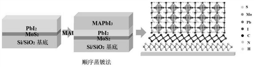
[0030] The invention provides a method for preparing a PVK-TMDCs van der Waals heterojunction, comprising the following steps:

[0031] (1) Prepare a transition metal chalcogenide thin film on a substrate by chemical vapor deposition;

[0032] (2) Preparing a perovskite film on the surface of the transition metal chalcogenide film obtained in the step (1) by physical vapor deposition to obtain a PVK-TMDCs van der Waals heterojunction.

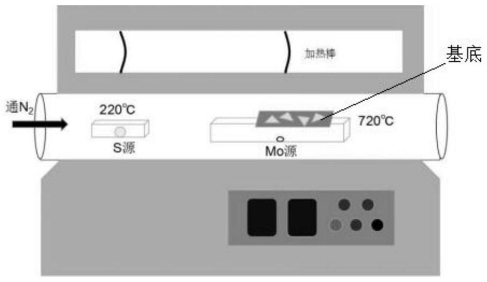
[0033] The invention adopts a chemical vapor deposition method to prepare a transition metal chalcogenide thin film on a substrate.

[0034] In the present invention, the material of the transition metal chalcogenide film is preferably MoS 2 、MoSe 2 or WS 2 , more preferably MoS 2 . The thin film prepared by the transition metal chalcogen compound in the invention has better photoelectric performance.

[0035] In the present invention, the substrate preferably includes a Si layer and SiO 2 layer; the Si layer is preferably a P-type heavi...

Embodiment 1

[0069] The substrate is Si layer and SiO 2 The composite material formed by layers, the Si layer is a P-type heavily doped Si layer, SiO 2 The thickness of the layer is 300nm; the transition metal chalcogenide is MoS 2 , the perovskite is MAPbI 3 ;

[0070] Pretreat the substrate. The pretreatment method is: cut the substrate along the crystal direction of the silicon substrate with a diamond glass knife, cut the substrate into a rectangle with a size of 3×2 cm, and first use deionized water to ultrasonically clean it for 15 minutes to remove debris on the surface of the substrate. ; Then ultrasonically clean with acetone for 15 minutes, isopropanol for 15 minutes, acetone for 15 minutes, and isopropanol for 15 minutes to remove the organic matter attached to the surface; finally, use hydrogen peroxide for 10 minutes to ultrasonically clean, and after cleaning, blow the surface of the substrate with a nitrogen gun dry to obtain a substrate with a clean surface;

[0071] Th...

Embodiment 2

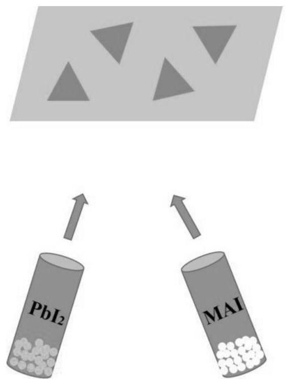
[0077] In the preparation method of Example 2, step (1), step (2) and step (3) are exactly the same as Example 1, the difference is that step (4) adopts co-evaporation method to deposit MAPbI 3 film;

[0078] (4) Deposition of MAPbI by co-evaporation 3 film, coated with a single layer of MoS with adhesive tape 2 The substrate is glued to the manipulator and then installed in the furnace. After the assembly is completed, the vacuum is started, and the mechanical pump is first turned on to pump the cavity to 10 -1 mbar, then turn on the molecular pump to pump the cavity to 10 -7 mbar; PbI 2 Raise to 340°C at a rate of 2°C / min, and raise MAI to 91°C at a rate of 0.5°C / min, and then use a robot to coat a single layer of MoS 2 The substrate is extended into the cavity, and the surface of the substrate is also facing down, and it is deposited for 3 minutes. 2 , and then open the cavity to take out the substrate to get MoS 2 -MAPbI 3 Heterojunction.


PUM

PropertyMeasurementUnit
thicknessaaaaaaaaaa

Abstract

The invention provides a PVK-TMDCs Van der Waals heterojunction and a preparation method thereof, and belongs to the technical field of photoelectric materials. A transition metal chalcogenide film is prepared on a substrate by adopting a chemical vapor deposition method; and a perovskite film is prepared on the surface of the transition metal chalcogenide film by adopting a physical vapor deposition method to obtain the PVK-TMDCs Van der Waals heterojunction. The transition metal chalcogenide film is prepared on the substrate by adopting a chemical vapor deposition method, the film with high purity, good compactness, small residual stress and good crystallization is obtained, then the perovskite film is prepared on the surface of the transition metal chalcogenide film by adopting a physical vapor deposition method, the transition metal chalcogenide film can regulate and control the growth structure and energy level of the perovskite film, impurities are prevented from appearing in a heterojunction interface, and the photoelectric detection performance of a photoelectric material is improved.

Description

technical field [0001] The invention relates to the technical field of photoelectric materials, in particular to a PVK-TMDCs van der Waals heterojunction and a preparation method thereof. Background technique [0002] Transition metal dichalcogenides (TMDCs, such as MoS 2 、MoSe 2 、WS 2 etc.) and perovskites (PVK, such as MAPbX 3 (X=I, Br, Cl), CsPbX 3 etc.) have good photoelectric performance, and the heterojunction formed by stacking them together has excellent photodetection performance. At present, this kind of heterojunction is mainly prepared by spin coating method or fixed-point transfer method, but the interface of the heterojunction prepared by these two methods is often not very clean, the repeatability of the experiment is low, and the fixed-point transfer method based on mechanical stripping Transfer technology cannot achieve mass production, which greatly affects the performance and application of subsequent devices. [0003] Therefore, it is necessary to p...

Claims


Application Information

Patent Timeline
Patent Type & Authority Applications(China)
IPC IPC(8): H01L31/18H01L31/032H01L31/0352H01L51/48H01L51/42H01L51/46
CPCH01L31/18H01L31/03529H01L31/032H10K71/00H10K71/164H10K85/30H10K30/10H10K2102/00Y02E10/549Y02P70/50
Inventor 黄寒邵子依郭晓肖君婷游思雯
Owner CENT SOUTH UNIV
Why Eureka
Try Eureka