Metal interconnection structure, semiconductor device and method for improving performance of diffusion barrier layer

A technology of metal interconnect structure and barrier layer, which is applied in the direction of semiconductor devices, semiconductor/solid-state device manufacturing, semiconductor/solid-state device components, etc., can solve the problems of interconnection metal and substrate reaction spikes, barrier characteristic degradation, etc.

Active Publication Date: 2021-04-13
INST OF MICROELECTRONICS CHINESE ACAD OF SCI
View PDF8 Cites 0 Cited by
  • Summary
  • Abstract
  • Description
  • Claims
  • Application Information

AI Technical Summary

Problems solved by technology

[0004] At present, a single-layer Co-based alloy can be used instead of the Ta / TaN double-layer structure, but when the Co-based alloy is used in the contact hole, after high temperature and long-term annealing, the barrier properties will be degraded, and the interconnection metal in the contact hole will easily react with the substrate. Spikes are formed, causing large leakage

Method used


Image

  • Metal interconnection structure, semiconductor device and method for improving performance of diffusion barrier layer
  • Metal interconnection structure, semiconductor device and method for improving performance of diffusion barrier layer
  • Metal interconnection structure, semiconductor device and method for improving performance of diffusion barrier layer

Examples


Embodiment Construction

[0023] Exemplary embodiments of the present disclosure will be described in more detail below with reference to the accompanying drawings. Although exemplary embodiments of the present disclosure are shown in the drawings, it should be understood that the present disclosure may be embodied in various forms and should not be limited by the embodiments set forth herein. Rather, these embodiments are provided for more thorough understanding of the present disclosure and to fully convey the scope of the present disclosure to those skilled in the art.

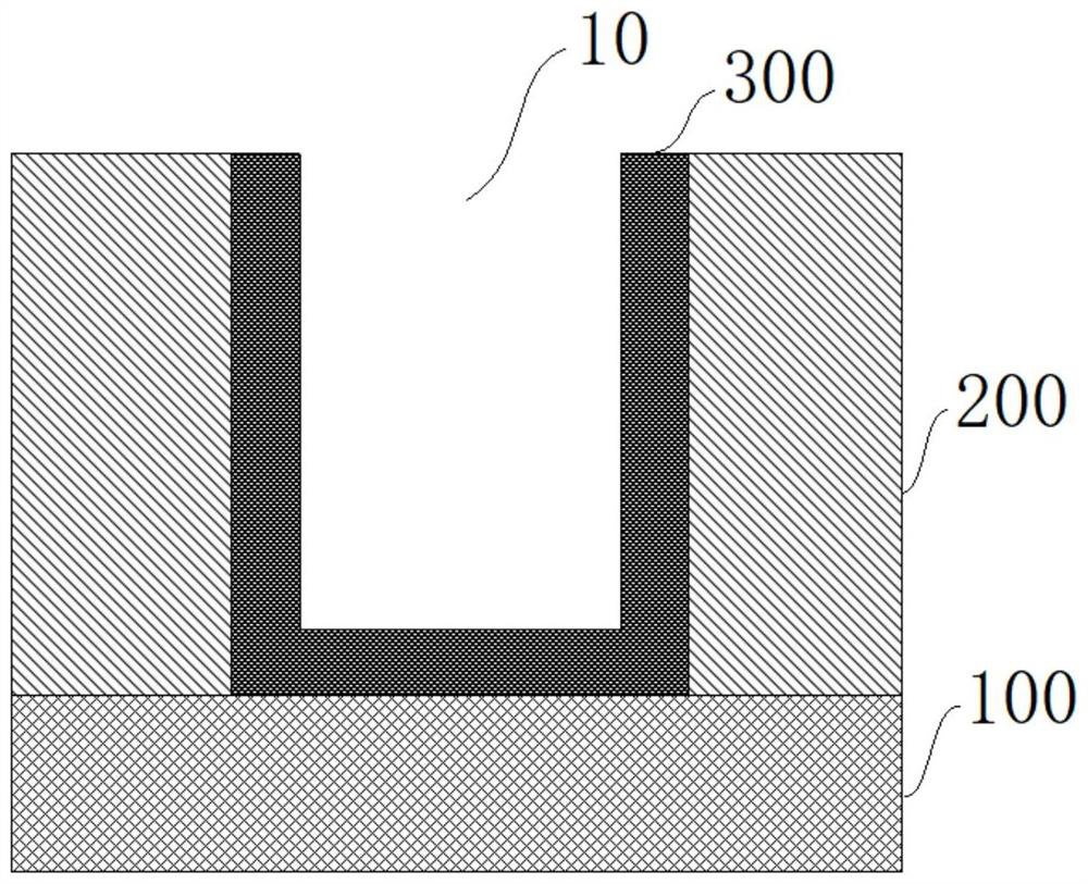
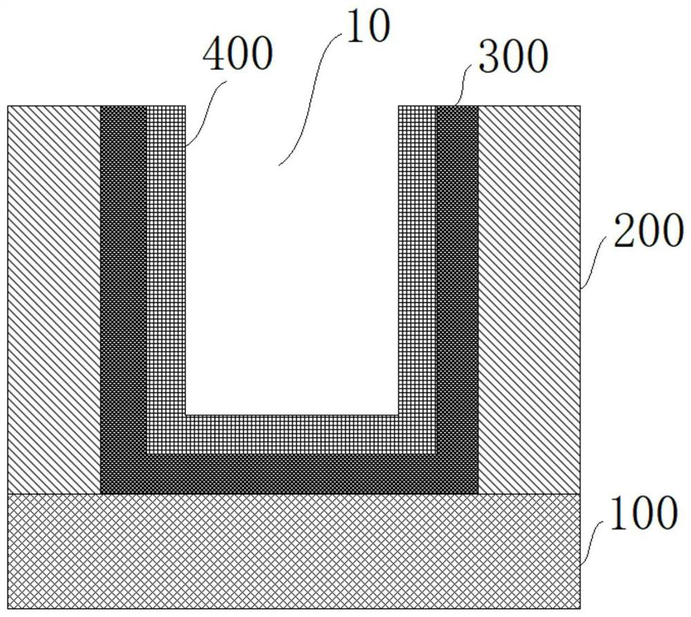
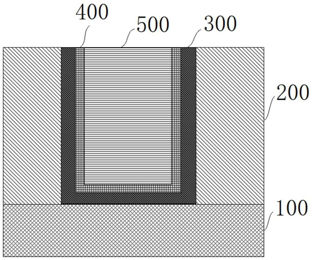
[0024] Figure 1d with Figure 2d Respectively show a cross-sectional view of a metal interconnection structure in a concept of the present invention; at the same time, Figure 1d It also shows a cross-sectional view of a partial structure of a semiconductor device in a concept of the present invention; Figure 2d A cross-sectional view of a partial structure of a semiconductor device in another concept of the present invention i...


PUM


Abstract

The invention provides a metal interconnection structure, a semiconductor device and a method for improving the performance of a diffusion impervious layer. The metal interconnection structure comprises an interconnection metal layer, a passivation layer and the diffusion impervious layer, wherein the passivation layer is connected between the interconnection metal layer and the diffusion impervious layer; the diffusion impervious layer is a Co-based alloy layer; and the passivation layer is formed by processing the surface of the diffusion barrier layer by using plasma. According to the metal interconnection structure, the diffusion impervious layer is arranged to be the Co-based alloy layer, so that the resistivity of the diffusion impervious layer can be reduced, and meanwhile, more effective volume can be reserved for an interconnection line; and the Co-based alloy layer is subjected to plasma treatment by using special gas, so that a passivation layer is formed on the surface of the Co-based alloy layer, and the barrier property is improved.

Description

technical field [0001] The invention relates to the technical field of semiconductors, in particular to a metal interconnection structure, a semiconductor device and a method for improving the performance of a diffusion barrier layer. Background technique [0002] As the device size reaches the process node of 5nm and below, the resistivity and thickness of the barrier layer material become the key factors affecting the resistance of the middle-end (MEOL) and back-end (BEOL) process interconnection lines, which seriously restricts the improvement of device performance. In the traditional process, Ta / TaN and Ti / TiN are mostly used as the diffusion barrier and adhesion layer, so as to ensure that the interconnection metal can grow without pores in the high aspect ratio via hole, the step coverage is good, and the metal ion is prevented from entering the dielectric layer. Medium diffusion, improved reliability and electromigration characteristics. At the same time, the thickne...

Claims


Application Information

Patent Timeline
Patent Type & Authority Applications(China)
IPC IPC(8): H01L23/528H01L23/532H01L21/768
CPCH01L23/528H01L23/53209H01L21/76831H01L2221/1057Y02P70/50
Inventor 张丹罗军许静叶甜春
Owner INST OF MICROELECTRONICS CHINESE ACAD OF SCI
Why Eureka
Try Eureka