Semiconductor wafer epitaxial growth device and working method thereof

An epitaxial growth and semiconductor technology, applied in crystal growth, single crystal growth, single crystal growth, etc., can solve the problem of limiting the detection system's recognition accuracy of defect types, affecting the uniformity of the temperature field on the wafer surface, and limiting the recognition accuracy of the detection system, etc. problem, to achieve the effect of ingenious device structure design, good working stability, and uniformity of temperature field

Pending Publication Date: 2021-04-16
东莞市中科汇珠半导体有限公司
View PDF9 Cites 1 Cited by
  • Summary
  • Abstract
  • Description
  • Claims
  • Application Information

AI Technical Summary

Problems solved by technology

However, in this method, only the reflection signal of the substrate to the laser is collected, and the monitoring device is inside the reaction chamber
This will lead to the following problems: 1) only the reflected light signal generated by the oblique incidence on the substrate surface will limit the detection accuracy of the detection system for the defect type; 2) placing the detection system in the reaction chamber will not only make the temperature field of epitaxial growth It is difficult to control, and requires strict thermal insulation protection for the detection system, especially for the case where a high-temperature epitaxial furnace is required to complete material growth (for example, the homoepitaxial growth of SiC, the temperature needs to be between 1500 ° C and 1700 ° C)
However, for practical application and detection of surface defects, this technical solution has the following problems: 1) Only the reflected light signal generated by normal incidence on the substrate surface, if used for surface defect detection, will limit the detection accuracy of the detection system for the type of defect; 2) The carrier plate on which the wafer is placed moves linearly along the direction parallel to the wafer surface, which will seriously affect the uniformity of the temperature field on the wafer surface during the actual epitaxial growth process

Method used


Image

  • Semiconductor wafer epitaxial growth device and working method thereof
  • Semiconductor wafer epitaxial growth device and working method thereof
  • Semiconductor wafer epitaxial growth device and working method thereof

Examples


Embodiment 1

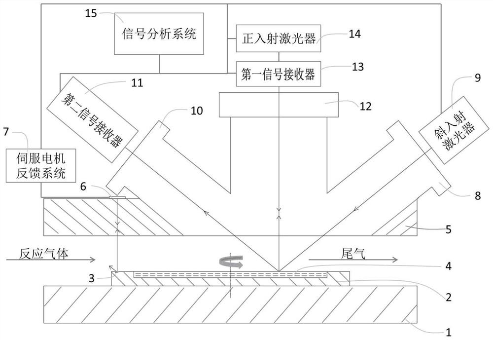
[0028] Embodiment 1: A semiconductor wafer epitaxial growth device and its working method provided in this embodiment, see figure 1 , figure 2 and image 3 , the semiconductor wafer epitaxial growth device includes an epitaxial growth system and an optical surface analysis system, wherein the epitaxial growth system includes a growth chamber and a graphite base 2, and the optical surface analysis system includes a graphite disk speed detector 6, a motor feedback system 7. Signal analysis system 15 , first signal receiver 11 , second signal receiver 13 , oblique incidence laser 9 and normal incidence laser 14 .

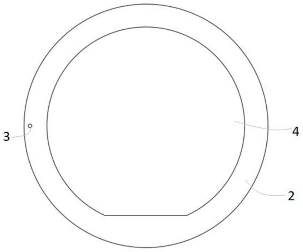
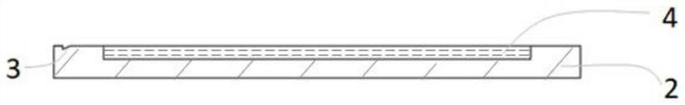
[0029] The graphite base 2 is arranged on the bottom 1 of the growth chamber, and the top 2 of the growth chamber is provided with a normal incidence window 12 facing the graphite base 2 and an oblique incidence window 8 obliquely facing the graphite base 2 and signal receiving window. The normal incidence window 12, the oblique incidence window 8 and the signal re...

Embodiment 2

[0042] Embodiment 2: This embodiment provides a semiconductor wafer epitaxial growth device and its working method, which are basically similar to Embodiment 1, except that a tantalum carbide coating is provided on the surface of the graphite base 2 .

[0043] When working, take the wafer substrate as an 8-inch Si wafer substrate as an example:

[0044] (1) Putting the wafer substrate into the graphite base 2 positioned in the growth chamber for in-situ etching of hydrogen and hydrogen chloride;

[0045] (2) Normal incidence laser 14 emits a laser beam perpendicular to the surface of the wafer substrate with a wavelength of 635nm to irradiate the wafer substrate. degree, but not perpendicular to the surface of the wafer substrate, a laser with a wavelength of 635nm is irradiated on the wafer substrate;

[0046] (3) The graphite base 2 drives the wafer substrate to rotate, and combines the normal incidence laser 14 and the oblique incidence laser 9 to perform translational mov...


PUM


Abstract

The invention discloses a semiconductor wafer epitaxial growth device and a working method thereof. The semiconductor wafer epitaxial growth device comprises an epitaxial growth system and an optical surface analysis system, wherein the epitaxial growth system comprises a growth cavity and a graphite base, the optical surface analysis system comprises a graphite disc rotating speed detector, a motor feedback system, a signal analysis system, an oblique incidence laser, a normal incidence laser, a first signal receiver and a second signal receiver. The graphite base drives the wafer to rotate, incident laser irradiation of the normal incident laser device and the oblique incident laser device is combined, laser signals are received through the first signal receiver and the second signal receiver and fed back to the signal processing system to be compared and analyzed, defect information on the whole surface of the wafer can be detected online more accurately in real time, therefore, real-time process parameter optimization is carried out according to the fed-back defect information, and the product yield is improved; and the optical surface analysis system adopts an outer side structure, is not influenced by high temperature and has good working stability.

Description

technical field [0001] The invention belongs to the technical field of semiconductors, and in particular relates to a semiconductor wafer epitaxial growth device and a working method thereof. Background technique [0002] Semiconductor wafers can obtain epitaxial layers with high quality, specific thickness and specific carrier concentration through epitaxial technology. For specific semiconductor and device types, specific epitaxial processes need to be developed to achieve the production of epitaxial wafers. The cycle and cost of epitaxial process development depend on the accuracy and effectiveness of process optimization. Only by feeding back the growth results caused by the process parameters as quickly as possible can the research and development cycle be shortened and the cost reduced to the greatest extent. This requires real-time online monitoring technology. Aiming at the above-mentioned technical problems, some related patents have been released to the public a...

Claims


Application Information

Patent Timeline
Patent Type & Authority Applications(China)
IPC IPC(8): C30B25/08C30B25/12C30B25/16C30B25/18C30B25/20C30B28/14C30B29/36H01L21/66H01L21/67
Inventor 杨军伟宋华平陈蛟黄敏王文军简基康陈小龙
Owner 东莞市中科汇珠半导体有限公司
Why Eureka
Try Eureka