Trench gate semiconductor device and manufacturing method thereof

A manufacturing method and trench gate technology are applied in the manufacture of trench gate semiconductor devices and in the field of trench gate semiconductor devices, which can solve problems such as restricting process development and manufacturing difficulties, and achieve step reduction and elimination of step limitations. Effect

Pending Publication Date: 2021-04-23
SHANGHAI HUAHONG GRACE SEMICON MFG CORP
View PDF5 Cites 1 Cited by
  • Summary
  • Abstract
  • Description
  • Claims
  • Application Information

AI Technical Summary

Problems solved by technology

[0016] but figure 2 In the shown structure, when reducing Rb by reducing d2, a new problem will appear: that is, as the pitch of the trench gate semiconductor device continues to shrink, figure 2 Among them, the step is the sum of the width d1 and the pitch of the gate trench. As the step shrinks, the design rule from the contact hole to the trench gate becomes more and more tight. For example, when the pitch is reduced to within 1 μm, Gate (Gate) critical dimension (CD) is figure 2 d1, CT CD in figure 2 There are great challenges in the design rule for the distance of d3 and CT to Gate, such as 0.3μm, 0.3μm and 0.3μm respectively to meet the requirement of 0.9μm, which is extremely difficult to manufacture
This also limits the further development of the process

Method used


Image

  • Trench gate semiconductor device and manufacturing method thereof
  • Trench gate semiconductor device and manufacturing method thereof
  • Trench gate semiconductor device and manufacturing method thereof

Examples


no. 1 example

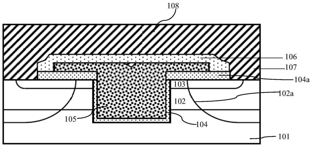
[0079] The trench gate semiconductor device of the first embodiment of the present invention:

[0080] Such as Figure 4 As shown, it is a schematic structural diagram of a trench gate semiconductor device in the first embodiment of the present invention; the trench gate semiconductor device in the embodiment of the present invention includes:

[0081] A body region 2 doped with a second conductivity type is formed in the first epitaxial layer 1 doped with the first conductivity type, the body region 2 extending downward from the top surface of the first epitaxial layer 1 .

[0082] The trench gate includes a gate trench 4 , a gate dielectric layer 5 and a gate conductive material layer 6 . In the first embodiment of the present invention, the gate dielectric layer 5 includes a gate oxide layer; the gate conductive material layer 6 includes a polysilicon gate.

[0083] The gate trench 4 passes through the body region 2 , and the top surface of the gate trench 4 is even with ...

no. 2 example

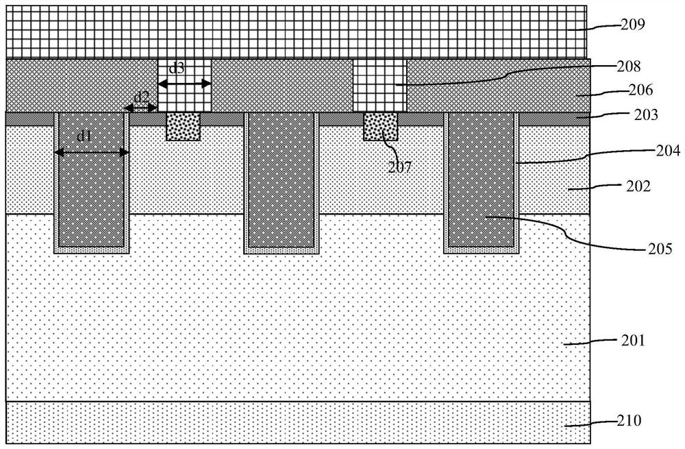
[0096] The trench gate semiconductor device of the second embodiment of the present invention:

[0097] Such as Figure 5 As shown, it is a schematic structural diagram of the trench gate semiconductor device of the second embodiment of the present invention; the difference between the trench gate semiconductor device of the second embodiment of the present invention and the trench gate semiconductor device of the first embodiment of the present invention is:

[0098] A super junction structure is formed in the first epitaxial layer 1 , and the super junction structure is formed by alternating columns 12 of the first conductivity type and the second conductivity type.

[0099] The first conductivity type columns are composed of the first epitaxial layer 1 between the second conductivity type columns 12; the second conductivity type columns 12 are composed of second conductivity type ion implantation regions or filled with The superjunction trench is composed of a second epita...


PUM


Abstract

The invention discloses a trench gate semiconductor device, which comprises a body region formed in a first epitaxial layer, a gate trench passing through the body region, a gate conductive material layer completely filling the bottom region of the gate trench, and a source region formed on the side surface of the top region of the gate trench through angled ion implantation self-alignment; a top dielectric layer is formed on the surface of the gate conductive material layer, and first grooves are formed in the vertex angles of the two sides of the top dielectric layer; the bottom of a source contact hole is formed on the surface of the top dielectric layer in each first groove and between the first grooves in a self-aligning manner; and the top surfaces of the source region in the first grooves are in contact with the side surface of the source contact hole to realize source region leading-out. The invention further discloses a manufacturing method of the trench gate semiconductor device. According to the invention, the alignment of transverse isolation between the source contact hole and the trench gate is not required, the stepping of the device can be reduced, the base resistance of a parasitic triode can be reduced, and the process window and the producibility can be improved at the same time.

Description

technical field [0001] The invention relates to the field of semiconductor integrated circuit manufacturing, in particular to a trench gate semiconductor device. The invention also relates to a manufacturing method of the trench gate semiconductor device. Background technique [0002] The conduction of the parasitic triode of the MOSFET can easily cause the MOSFET to burn out, which has a great impact on the durability of the MOSFET. The main method to suppress the turn-on of the parasitic triode is to reduce the base parasitic resistance (Rb) of the parasitic triode, so as to ensure that the device can withstand greater avalanche energy under the condition of unclamped inductive switching (UIS). [0003] The first existing trench gate semiconductor device: [0004] One way to reduce Rb is to increase the doping concentration on the Rb path, such as figure 1 As shown, it is a schematic structural diagram of the first existing trench gate semiconductor device; taking the N...

Claims


Application Information

Patent Timeline
Patent Type & Authority Applications(China)
IPC IPC(8): H01L29/78H01L29/739H01L29/06H01L21/336H01L21/331
CPCH01L29/7813H01L29/7397H01L29/0634H01L29/66348H01L29/66734
Inventor 李昊
Owner SHANGHAI HUAHONG GRACE SEMICON MFG CORP
Why Eureka
Try Eureka