
Method for preparing perovskite QLED electron transport layer by transferring ZnO nano-film

A technology of electron transport layer and nano-thin film, which is applied in the direction of circuits, electrical components, electric solid devices, etc., to achieve the effect of reducing damage and making the process simple and easy to operate

Active Publication Date: 2021-04-23
FUZHOU UNIV +1
View PDF7 Cites 2 Cited by
  • Summary
  • Abstract
  • Description
  • Claims
  • Application Information

AI Technical Summary

Problems solved by technology

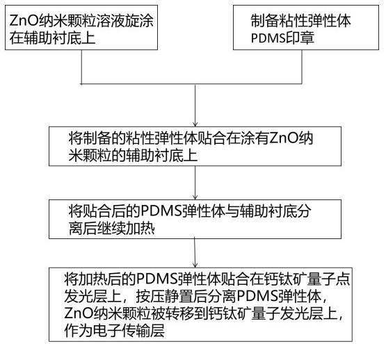
[0004] Aiming at the problem that the electron transport layer of the perovskite quantum dot light-emitting diode is difficult to realize by the solution method, the purpose of the present invention is to provide a method for transferring the ZnO nano film to prepare the electron transport layer of the perovskite QLED. The spin-coated nano-ZnO film is adsorbed, then heated to weaken the viscosity and then transferred to the perovskite quantum dot light-emitting layer, the PDMS is separated from the ZnO layer, and the ZnO nano-film is transferred to the perovskite quantum dot light-emitting layer. The method of the present invention can Effectively reduce solvent damage to the light-emitting layer of perovskite quantum dots, and build an ideal heterogeneous interface

Method used


Image

  • Method for preparing perovskite QLED electron transport layer by transferring ZnO nano-film
  • Method for preparing perovskite QLED electron transport layer by transferring ZnO nano-film

Examples


Embodiment 1

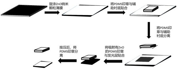
[0028] Schematic diagram of the process flow of a method of transferring ZnO nanoparticles to prepare the electron transport layer of perovskite QLED, as shown in figure 1 shown. Specifically include the following steps:

[0029] (1) First prepare the elastomeric PDMS stamp: coat a layer of polydimethylsiloxane (PDMS) on the glass substrate, and the area of ​​the PDMS stamp is 1cm 2 And the thickness is 7mm, and then it is heated for 20 minutes to make it in an incompletely cured state with viscosity, and the annealing temperature is 80°C.

[0030] Among them, PDMS is mixed with a liquid component and a curing agent in a mass ratio of 10:1, and then stirred for 10 minutes, then put it in a vacuum drying oven to evacuate it, and take it out after standing for 0.5 hours, and discharge the dissolved air.

[0031] (2) Preparation of ZnO nanoparticle solution, first dissolve 0.59g of zinc acetate in 25ml of methanol, then heat and stir in a water bath with a temperature of 63°C-6...

Embodiment 2

[0035] (1) Preparation of elastomeric PDMS stamp: Coating a layer of polydimethylsiloxane (PDMS) on polyethylene terephthalate (PET), the area of ​​the PDMS stamp is 1cm 2 And the thickness is 7mm, and then it is heated for 20 minutes to make it in an incompletely cured state with viscosity, and the annealing temperature is 80°C.

[0036] Among them, PDMS is mixed with a liquid component and a curing agent in a mass ratio of 10:1, then stirred for 10 minutes, then put it in a vacuum drying oven to evacuate it, let it stand for 0.5 hours, and then take it out to discharge the dissolved air.

[0037] (2) Preparation of ZnO nanoparticle solution, first dissolve 0.59g of zinc acetate in 25ml of methanol, then heat and stir in a water bath with a temperature of 63°C-65°C. At the same time, dissolve 0.3g of potassium hydroxide in 13ml of methanol, heat in a water bath at the same temperature for 5 minutes, then drop the potassium hydroxide solution into the zinc acetate solution, an...


PUM


Abstract

The invention belongs to the technical field of electron transport layer QLED preparation, and particularly relates to a method for preparing a perovskite QLED electron transport layer by transferring a ZnO nano-film through a dry process. The method comprises the following steps: preparing a layer of ZnO nano-film on an auxiliary substrate, attaching a pre-prepared viscous elastomer PDMS to the ZnO nano-film, adsorbing the ZnO nano-film by utilizing the viscosity of the elastomer PDMS, and separating PDMS / ZnO from the auxiliary substrate; and annealing to weaken the viscosity of the PDMS stamp, attaching PDMS / ZnO to a perovskite quantum dot light-emitting layer, pressing, transferring ZnO nanoparticles to the perovskite layer, and finally separating the PDMS stamp from the ZnO layer. According to the invention, the ZnO nano-film is transferred to the perovskite quantum dot light-emitting layer through the PDMS stamp to be used as an electron transport layer, so that a perfect heterogeneous interface can be constructed, and the perovskite quantum dot light-emitting layer can be prevented from being damaged by a solvent effect in solution addition or a heat effect of a vacuum process.

Description

technical field [0001] The invention belongs to the technical field of electron transport layer QLED preparation, and in particular relates to a method for preparing a perovskite QLED electron transport layer by dry transferring a ZnO nano film. Background technique [0002] Zinc oxide is a direct bandgap semiconductor with a bandgap of 3.37eV, and its exciton binding energy can reach 60meV at room temperature. The crystal structure of ZnO is generally hexagonal wurtzite structure, which has excellent optical and electrical properties. The intrinsic defects of nano-zinc oxide are mainly Zn gaps and O vacancies, and zinc oxide is an n-type semiconductor material, which is commonly used in the electron transport layer of quantum dot light-emitting diodes. [0003] Perovskite quantum dots have shown attractive application prospects in perovskite light-emitting diodes (PeLEDs) due to their excellent optoelectronic properties. At present, PeLED devices prepared with perovskite q...

Claims


Application Information

Patent Timeline
IPC IPC(8): H01L51/50H01L51/56H01L51/00
Inventor 胡海龙李福山孟汀涛井继鹏高宏锦郭太良
Owner FUZHOU UNIV
Learn More