Preparation method of phase change memory based on nano current channel

A phase change memory and current channel technology, applied in the field of phase change memory, can solve the problems of high process cost and difficulty, and achieve the effects of simple process, low total energy and volume reduction

Active Publication Date: 2021-04-27
HUAZHONG UNIV OF SCI & TECH
View PDF14 Cites 1 Cited by
  • Summary
  • Abstract
  • Description
  • Claims
  • Application Information

AI Technical Summary

Problems solved by technology

[0007] Aiming at the defects of the prior art, the present invention provides a method for preparing a phase-change memory based on a nano-current channel. problems, and increase the current density in the contact area,

Method used


Image

  • Preparation method of phase change memory based on nano current channel
  • Preparation method of phase change memory based on nano current channel
  • Preparation method of phase change memory based on nano current channel

Examples


preparation example Construction

[0052] The preparation method of the phase-change memory based on the nano-current channel provided by the present invention includes:

[0053] (1) growing the first electrode layer on the substrate;

[0054] (2) depositing and growing an insulating layer on the first electrode layer;

[0055] (3) Etching the insulating layer up to the first electrode layer and forming a groove whose bottom surface is a metal electrode layer by using a photolithography etching process;

[0056] (4) preparing a nano current channel layer with metal grains in the groove, and the metal grains run through the thickness of the layer;

[0057] (5) Depositing a phase change material above the nano current channel layer;

[0058] (6) Depositing a second electrode layer on the phase change material to form a phase change memory with a nano current channel layer.

[0059] The present invention can adopt magnetron sputtering method, chemical vapor deposition method, plasma enhanced chemical vapor depo...

Embodiment 1

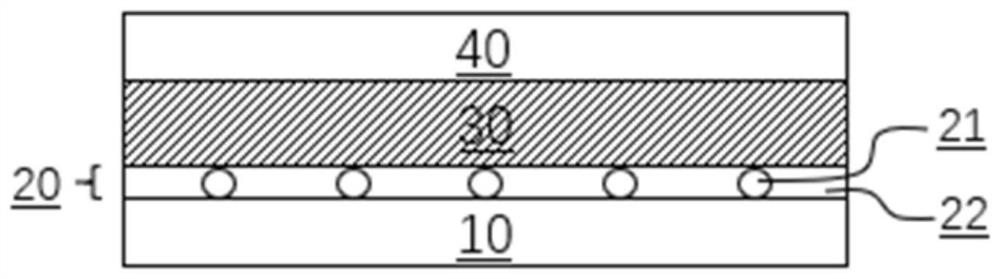
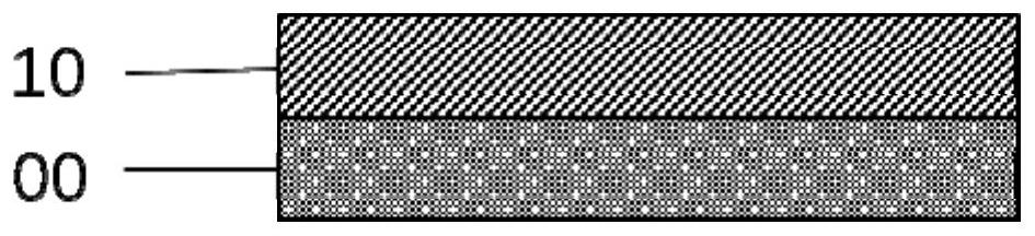
[0078] According to the first embodiment of the present invention, a cross-sectional view of an exemplary structure of a phase-change memory with a nanometer current channel layer and figure 2 show. The bottom electrode 10 is formed on SiO 2 On the substrate, the material of the bottom electrode 10 is selected from W, Pt, Au, Al, Cu, Ti, Ta and other metal materials and conductive materials of their alloys. The nano-current channel 20 is formed on the bottom electrode 10, the nano-current channel layer 20 is composed of an insulating and heat-insulating material 22 and conductive nano-crystal grains 21 embedded in the middle of the insulating and heat-insulating material layer, wherein the thickness of the nano-current channel layer 20 is between 1nm and 30nm . The size of the conductive nanoparticles in the insulating layer is 1nm-30nm, and the size of the conductive nanoparticles 21 in the direction perpendicular to the film is not less than the thickness of the nano curr...

Embodiment 2

[0081] According to the second embodiment of the present invention, the finite element simulation is performed on the phase-change memory structure with the nano current channel layer and the writing process of the traditional phase-change memory structure.

[0082] The simulation adopts the simplest three-layer phase-change memory cell structure in Embodiment 1. The material parameters used in the simulation are listed in Table 1 (the thermal and electrical parameters of various materials used in the finite element analysis). The upper and lower electrode materials of the two cell structures are Pt, and the insulating layer material is SiO 2 And the phase change layer material is Ge 2 Sb 2 Te 5 , the thickness of the upper and lower electrodes, insulating layer, and phase change layer are all 100nm, and the diameter of the unit device is 100nm. 2 Material, using Ag as the nano current channel, its diameter is 6nm. A RESET current pulse with an amplitude of 60uA and a puls...


PUM

PropertyMeasurementUnit
Thicknessaaaaaaaaaa
Thicknessaaaaaaaaaa
Depthaaaaaaaaaa

Abstract

The invention discloses a preparation method of a phase change memory based on a nano current channel. The preparation method comprises the following steps of growing a first electrode layer on a substrate; depositing and growing an insulating layer on the first electrode layer; etching the insulating layer to the first electrode layer by using a photoetching process, and forming a groove of which the bottom surface is a metal electrode layer; preparing a nano current channel layer with metal crystal grains in the groove, wherein the metal crystal grains penetrate through the thickness of the layer; depositing a phase change material above the nano current channel layer; and depositing a second electrode layer above the phase change material to form the phase change memory with the nano current channel layer. According to the method, the contact area between the phase change layer and the electrode layer is greatly reduced through the nanoscale conductive channel, the current density of a local contact part is greatly improved, and heat production efficiency of current in the phase change layer is improved; electric heating utilization efficiency of the phase change layer is improved; and the process is simple, so operation power consumption of the phase change memory can be easily reduced.

Description

technical field [0001] The invention belongs to the technical field of phase-change memory, and more specifically relates to a preparation method of a phase-change memory based on a nanometer current channel. Background technique [0002] With the advent of the information age, memory plays an increasingly important role in our daily life. At present, research on memory has been developing in the direction of high speed, low power consumption, and high stability. Among them, the phase change memory (PCRAM) made by utilizing the phase change property of materials has great potential in the semiconductor market. [0003] The basic principle of phase-change memory is that phase-change materials can be reversibly switched between crystalline and amorphous states, and use the huge difference in resistance between different states of the material to realize "1" and "0" data storage. The commonly used phase-change materials are chalcogenides. By controlling the amplitude and pulse...

Claims


Application Information

Patent Timeline
IPC IPC(8): H01L45/00
CPCH10N70/231H10N70/801H10N70/011Y02D10/00
Inventor 程晓敏李瀚曾运韬朱云来刘香君缪向水
Owner HUAZHONG UNIV OF SCI & TECH
Why Eureka
Try Eureka