Method for improving light-emitting efficiency of light-emitting diode
A technology of light-emitting diodes and luminous efficiency, which is applied in the direction of electrical components, circuits, semiconductor devices, etc., can solve the problems affecting the luminous efficiency of devices, and achieve the effect of improving luminous efficiency, coupling efficiency and charge injection efficiency
- Summary
- Abstract
- Description
- Claims
- Application Information
AI Technical Summary
Problems solved by technology
Method used
Image
Examples
Embodiment 1
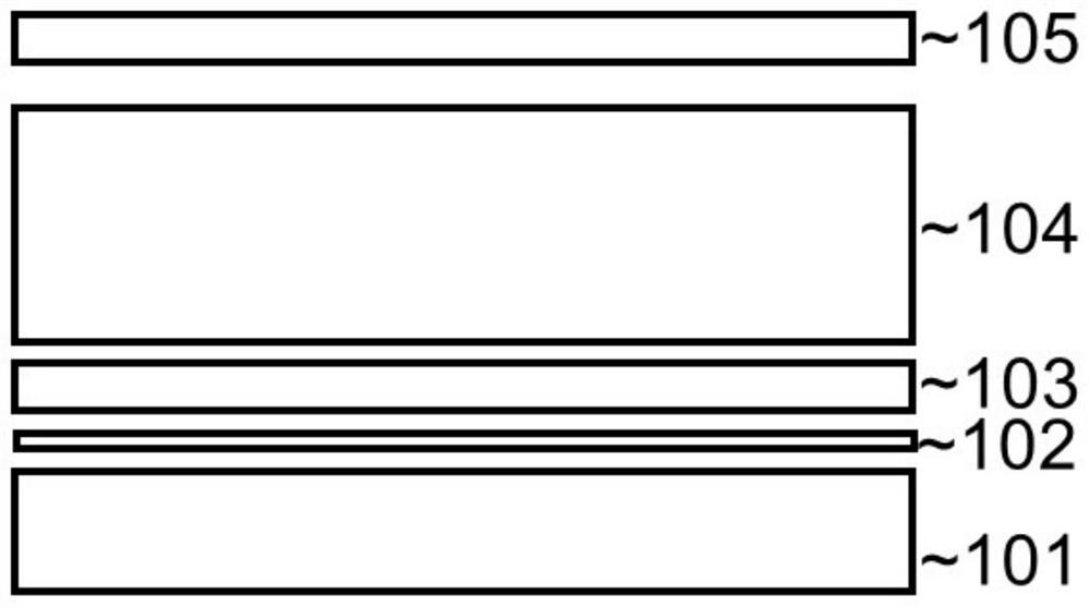
[0022] Such as figure 1 As shown, in this embodiment, the light-emitting diode has a bottom-emitting structure, and the anode uses a single-layer graphene 102 on the surface of a polyethylene terephthalate (PET) transparent substrate 101 as a transparent electrode. Use anti-reflection dopant film 103 (its thickness is 10 nanometers) between anode and luminescent layer 104, and the composition of this film is tetrapentafluorophenylboronic acid or other light transmittances 80~100% have anti-reflection effect p-type dopant, the cathode uses an aluminum thin film 105 (thickness is 100 nanometers), and the aluminum thin film 105 is located on the light emitting layer 104. An anti-reflective dopant film, a light-emitting layer and an aluminum film cathode are sequentially formed on the surface of the single-layer graphene anode. The tetrapentafluorophenylboronic acid thin film simultaneously improves the light extraction rate of the light-emitting layer on the anode side and the h...
Embodiment 2
[0024] The difference from Example 1 is:
[0025] Such as figure 2 As shown, in the present embodiment, the light-emitting diode is a top-emitting structure, the aluminum film 202 (its thickness is 150 nanometers) on the surface of the glass transparent substrate 201 is used as the transparent cathode at the bottom, and the carbon nanotube film 205 (its thickness is 10 nanometers) is used. ) as the top transparent anode. A light-emitting layer 203, a tetrapentafluorophenylboronic acid film 204 and a carbon nanotube film transparent anode are sequentially formed on the surface of the aluminum film cathode, and the external quantum efficiency of the light-emitting diode is 20%.
Embodiment 3
[0027] The difference from Example 1 is:
[0028] In this embodiment, the light-emitting diode is a fully transparent structure, and the anode adopts a single-layer graphene on the surface of a polyethylene terephthalate (PET) transparent substrate as a transparent electrode, and the cathode adopts a carbon nanotube film (its thickness is 8 nanometers). ). A tetrapentafluorophenylboronic acid film, a light-emitting layer and a carbon nanotube film cathode are sequentially formed on the surface of the single-layer graphene anode, and the external quantum efficiency of the light-emitting diode reaches 30%.
[0029] The results of the examples show that the method of the present invention introduces an anti-reflection dopant film between the transparent electrode and the light-emitting layer, and simultaneously improves the light outcoupling efficiency and charge injection efficiency of the transparent electrode through the anti-reflection dopant film, thereby improving the light...
PUM
| Property | Measurement | Unit |
|---|---|---|
| thickness | aaaaa | aaaaa |
| transmittivity | aaaaa | aaaaa |
| external quantum efficiency | aaaaa | aaaaa |
Abstract
Description
Claims
Application Information
 - R&D
- Intellectual Property
- Life Sciences
- Materials
- Tech Scout
- Unparalleled Data Quality
- Higher Quality Content
- 60% Fewer Hallucinations
Browse by: Latest US Patents, China's latest patents, Technical Efficacy Thesaurus, Application Domain, Technology Topic, Popular Technical Reports.
© 2025 PatSnap. All rights reserved.Legal|Privacy policy|Modern Slavery Act Transparency Statement|Sitemap|About US| Contact US: help@patsnap.com


