A method for improving blind hole pad removal of multi-level circuit boards and multi-level circuit boards

A technology of circuit boards and blind holes, which is applied in multi-layer circuit manufacturing, printed circuits, printed circuits, etc., can solve the problems of poor pad release and small thickness-to-diameter ratio of blind holes, etc., so as to solve the problems of pad release and open circuit, and improve production Efficiency, the effect of reducing medium thickness

Active Publication Date: 2022-06-07
珠海崇达电路技术有限公司 +1
View PDF4 Cites 0 Cited by
  • Summary
  • Abstract
  • Description
  • Claims
  • Application Information

AI Technical Summary

Problems solved by technology

[0004] The present invention aims at the above-mentioned existing technical defects, and provides a method for improving the blind holes of multi-level circuit boards. The hole connection composition, according to the manufacturing method of the laser blind hole, can reduce the interlayer thickness of the blind hole, so that the thickness-to-diameter ratio of the blind hole becomes smaller, which is beneficial to the copper plating of the blind hole, and improves the reliability of the blind hole. Solved the problem of poor opening of blind holes due to excessive interlayer thickness.

Method used


Image

  • A method for improving blind hole pad removal of multi-level circuit boards and multi-level circuit boards
  • A method for improving blind hole pad removal of multi-level circuit boards and multi-level circuit boards

Examples


Embodiment

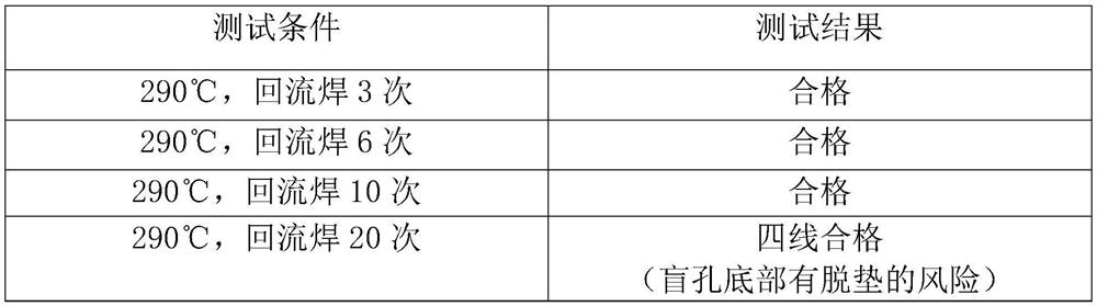
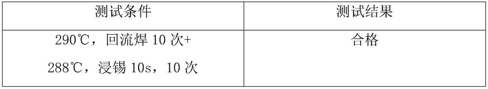
[0033] The manufacturing method of a third-order circuit board shown in this embodiment includes the following processing steps in sequence:

[0034] (1) Cutting material: cut out the core board according to the size of the jigsaw panel of 520mm×620mm, the thickness of the core board is 0.5mm (excluding the thickness of the outer layer copper), and the thickness of the outer layer copper surface of the core board is 0.5oz (1oz≈35μm) .

[0035] (2) Drilling in the inner layer: According to the existing drilling technology, the plug holes to be filled with resin are drilled on the core board according to the design requirements.

[0036] (3) Immersion copper, full-board electroplating: metallize the plug holes on the core board.

[0037] (4) Plating holes: paste the film on the core board, open the window at the position of the plug hole through exposure and development to form a plated hole pattern, and then electroplate the plug hole to thicken the copper layer in the hole, s...


PUM


Abstract

The invention discloses a method for improving blind hole degassing of a multi-stage circuit board and a multi-stage circuit board. The method includes the following steps: drilling a plug hole on a core board and metallizing the plug hole, then filling the plug hole with resin, and using an abrasive belt Metallize the surface of the resin after grinding the board; make the inner layer circuit on the core board; press the core board and copper foil into the first sub-board; drill the first blind hole and the first-order blind hole on the first sub-board, The first blind hole and the first-order blind hole are filled and leveled; the first sub-board and copper foil are pressed into the second sub-board; the second blind hole and the second-order blind hole are drilled on the second sub-board with controlled depth, and the second Blind holes and second-order blind holes are filled and leveled; the second sub-board and copper foil are pressed into a production board; third-order blind holes and through-holes are drilled on the production board with controlled depth, so that the third-order blind holes and through-hole metal Chemical; sequentially carry out subsequent processes on the production board to make a multi-level circuit board. The method of the invention can reduce the interlayer thickness of the blind hole, reduce the thickness-to-diameter ratio of the blind hole, and solve the problem that the blind hole is poorly opened due to excessive interlayer thickness.

Description

technical field [0001] The invention relates to the technical field of printed circuit board manufacturing, in particular to a method for improving the release of blind holes of a multi-level circuit board and a multi-level circuit board. Background technique [0002] The third-order laser HDI board is mainly used in the digital keyboard control box security module of the ATM machine. There are 2 pieces of PCBA in the keyboard control box, one of which is the keyboard touchpad, and the other is the safety control board under the touchpad. The working principle of the safety control board is: There are safety induction keys at both ends of the PCBA to connect with the ATM machine. When there is external damage / mechanical intrusion, the device senses and transmits the intrusion signal to the safety control core, and the BGA starts the self-destruction mode and formats the memory. , ATM automatically shuts down and cannot be restarted. The purpose of this board belongs to the ...

Claims


Application Information

Patent Timeline
Patent Type & Authority Patents(China)
IPC IPC(8): H05K3/42H05K3/46
CPCH05K3/429H05K3/4652H05K2201/09536
Inventor 孙保玉宋建远戴勇
Owner 珠海崇达电路技术有限公司
Why Eureka
Try Eureka