Processing method of thick copper PCB with step position containing bonding structure

A PCB board and processing method technology, applied in the field of thick copper PCB board processing, can solve the problems of difficult surface treatment, small pad-to-pad spacing, and inability to bond, so as to improve product yield and dense pads , to achieve the effect of bonding

Active Publication Date: 2021-05-07
深圳市辉煌线路板有限公司
View PDF6 Cites 1 Cited by
  • Summary
  • Abstract
  • Description
  • Claims
  • Application Information

AI Technical Summary

Problems solved by technology

[0002] With the continuous development of electronic technology, there will be more and more printed circuit boards that require bonding structures and are used for storage function requirements, and bonding positions are generally regular rectangular arrays, mostly square and circular bonding Welding pads have the characteristics of small spacing between pads, dense pads, and difficult surface treatment. At present, the widely used SMT chip technology is to solder the solder feet of the chip on the circuit board. This production process is not suitable In the processing of storage products, there are likely to be functional problems such as virtual soldering, false soldering, and missing soldering in the packaging test, and the advantage of the bonding method is that the finished product is anti-corrosion, earthquake-resistant and stable, while the conventional bonding structure The completed copper thickness is less than 35UM, and the thick copper plate is greater than 35UM, which is much higher than the traditional SMT placement method, but for some special structures, the bonding structure similar to data transmission requires high power, resulting in a thick base copper, but for Ordinary bonding production methods are unsatisfactory. During the lamination process, it is easy to form glue shortage and overflow, which leads to uncontrollability. The bonding chip is to bond the chip soldering feet to the printed circuit board through gold wire or tin wire. Pad bonding, there is glue on the pad or lack of glue around the pad, which will lead to failure of bonding or weak bonding

Method used


Image

  • Processing method of thick copper PCB with step position containing bonding structure
  • Processing method of thick copper PCB with step position containing bonding structure
  • Processing method of thick copper PCB with step position containing bonding structure

Examples


Embodiment Construction

[0037] In order to facilitate the understanding of the present invention, the present invention will be described in more detail below in conjunction with the accompanying drawings and specific embodiments. Preferred embodiments of the invention are shown in the accompanying drawings. However, the present invention can be implemented in many different forms and is not limited to the embodiments described in this specification. On the contrary, these embodiments are provided to make the understanding of the disclosure of the present invention more thorough and comprehensive.

[0038] Unless otherwise defined, all technical and scientific terms used in this specification have the same meaning as commonly understood by one of ordinary skill in the technical field of the invention. The terms used in the description of the present invention in this specification are only for the purpose of describing specific embodiments, and are not used to limit the present invention.

[0039] ...


PUM

PropertyMeasurementUnit
Thicknessaaaaaaaaaa

Abstract

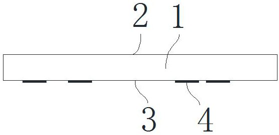
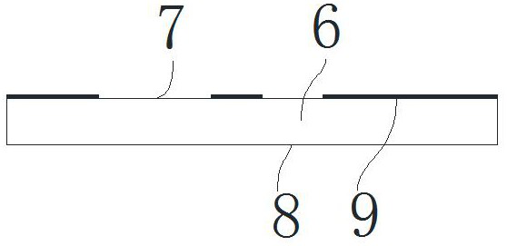
The invention provides a processing method for a thick copper PCB with a step position containing a bonding structure. The method comprises the steps that lamination design is carried out, and a lamination structure comprises a first core board, auxiliary filling glue, and a second core board; the first core board, the second core board and an auxiliary core board are cut according to the same longitude and latitude; the first core board is divided into two surfaces, one surface is an L1 layer, the other surface is an L2 layer, the second core board is divided into two surfaces, one surface is an L3 layer, and the other surface is an L4 layer; a circuit is manufactured on a press-fit corresponding surface, and auxiliary glue filling is carried out, namely a bonding structure area is hollowed out; the first core board, a non-flowing glue PP sheet, the first auxiliary glue body, the auxiliary core board, the second auxiliary glue body, a non-flowing glue PP sheet and the second core board are stacked in sequence, fixed through rivet holes and then pressed; then drilling, copper deposition, outer layer pattern, pattern electroplating, etching, resistance welding, character processing, surface treatment, forming, testing and final inspection processes are carried out; the L1 layer of the depth control gong faces upwards, and a bonding pad is exposed out of the bonding position of the depth control hollowed-out part.

Description

technical field [0001] The invention relates to a method for manufacturing a multilayer printed circuit board, in particular to a method for processing a thick copper PCB board with a bonding structure at the step position. Background technique [0002] With the continuous development of electronic technology, there will be more and more printed circuit boards that require bonding structures and are used for storage function requirements, and bonding positions are generally regular rectangular arrays, mostly square and circular bonding Welding pads have the characteristics of small spacing between pads, dense pads, and difficult surface treatment. At present, the widely used SMT chip technology is to solder the solder feet of the chip on the circuit board. This production process is not suitable In the processing of storage products, there are likely to be functional problems such as virtual soldering, false soldering, and missing soldering in the packaging test, and the adv...

Claims


Application Information

Patent Timeline
IPC IPC(8): H05K3/46H05K3/34
CPCH05K3/46H05K3/34
Inventor 黄海辉白云飞
Owner 深圳市辉煌线路板有限公司
Why Eureka
Try Eureka