Manufacturing method of LED chip and product thereof
A technology of LED chip and manufacturing method, which is applied in semiconductor/solid-state device manufacturing, electrical components, circuits, etc., and can solve problems such as low process yield and wafer edge warping
- Summary
- Abstract
- Description
- Claims
- Application Information
AI Technical Summary
Problems solved by technology
Method used
Image

Examples
Embodiment 1
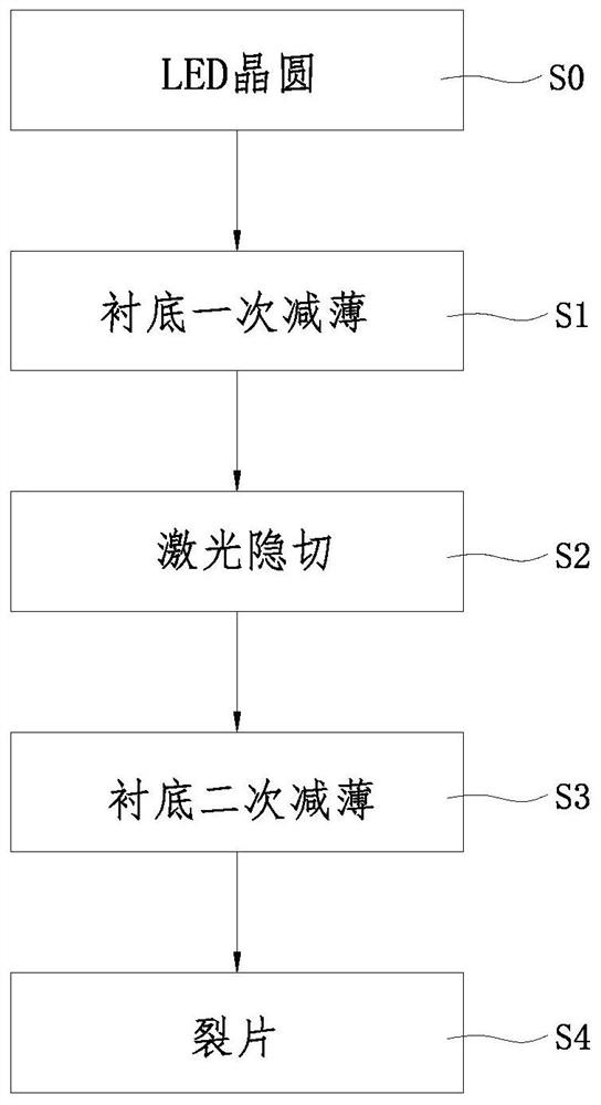
[0041] This embodiment provides a method for manufacturing an LED chip, such as figure 1 shown, including:
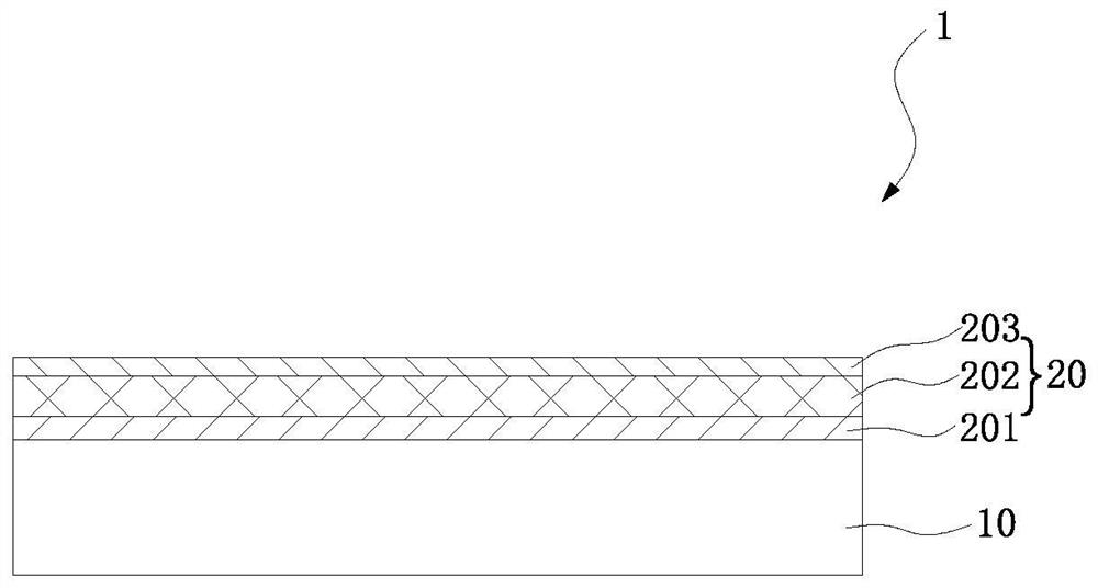
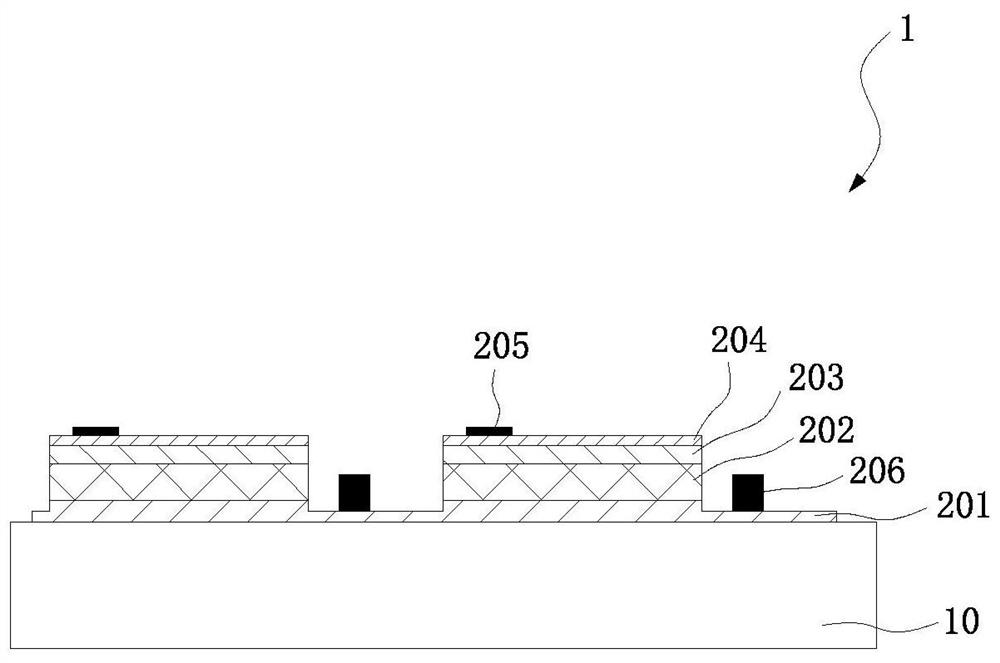
[0042] Step S0: providing an LED wafer (wafer), which includes a substrate and a plurality of epitaxial units on the substrate, each of which includes an epitaxial structure and electrodes on the epitaxial structure.
[0043] Wherein, the substrate may be a sapphire substrate, a silicon carbide substrate or a gallium nitride substrate or the like. In this embodiment, the substrate is a sapphire substrate, and the epitaxial structure is grown on the c-plane surface of the sapphire substrate.
[0044] The epitaxial structure at least includes a first conductivity type semiconductor layer, an active layer and a second conductivity type semiconductor layer stacked sequentially on the substrate. For example, in this embodiment, the first conductivity type semiconductor layer is an N-type nitride layer, the active layer is a GaN-based quantum well layer, and the second cond...
Embodiment 2
[0062] This embodiment also provides a method for manufacturing an LED chip, which is roughly the same as the method in Embodiment 1. Refer to Figure 8 ,include:
[0063] Step S0: providing an LED wafer (wafer), which includes a substrate and a plurality of epitaxial units on the substrate, each of which includes an epitaxial structure and electrodes on the epitaxial structure.
[0064] Step S1: first thinning the side of the substrate away from the epitaxial structure, so that the thickness of the substrate is reduced to a first thickness L1.
[0065] Step S2: Stealth dicing is performed on the substrate to form multiple laser scratches in the substrate, each laser scratch is positioned between two adjacent epitaxial units to define the size of the LED chip.
[0066] Step S3: performing a second thinning on the side of the substrate facing away from the epitaxial structure, so as to reduce the thickness of the substrate to the target thickness L2.
[0067] The above steps ...
Embodiment 3
[0073]This embodiment also provides a method for manufacturing an LED chip, which is substantially the same as that in Embodiment 1 or Embodiment 2, the difference being that the epitaxial structure in Embodiment 1 or Embodiment 2 is an InGaN system , which is directly grown on the c-plane surface of the sapphire substrate by means of epitaxy. However, the epitaxial structure in this embodiment is AlGaInP system, and the AlGaInP system epitaxial structure is first grown on the gallium arsenide substrate, and then the AlGaInP system epitaxial structure is transferred to the sapphire substrate by means of transfer.
[0074] Specifically, refer to Figure 11 , Figure 11 It is a gallium arsenide substrate and an AlGaInP epitaxial structure on its surface, wherein the AlGaInP epitaxial structure at least includes an N-type semiconductor layer, an active layer and a P-type semiconductor layer sequentially formed on the substrate surface. exist Figure 11 Among them, reference nu...
PUM
| Property | Measurement | Unit |
|---|---|---|
| Thickness | aaaaa | aaaaa |
| Thickness | aaaaa | aaaaa |
| Thickness | aaaaa | aaaaa |
Abstract
Description
Claims
Application Information