Charged particle beam drawing device, charged particle beam drawing method, and program

A technology of charged particle beams and drawing devices, which is applied in the direction of exposure devices, circuits, discharge tubes, etc. in the photolithography process, can solve the problems of insufficient dimensional accuracy, and achieve the effect of high precision position offset

Pending Publication Date: 2021-05-25
NUFLARE TECH INC
View PDF15 Cites 0 Cited by
  • Summary
  • Abstract
  • Description
  • Claims
  • Application Information

AI Technical Summary

Problems solved by technology

However, in the conventional electrification correction, there is a problem that the dimensional accuracy required recently cannot be adequately met in a part of the area.

Method used


Image

  • Charged particle beam drawing device, charged particle beam drawing method, and program
  • Charged particle beam drawing device, charged particle beam drawing method, and program
  • Charged particle beam drawing device, charged particle beam drawing method, and program

Examples


Embodiment Construction

[0028] Embodiments of the present invention will be described below based on the drawings. In the embodiment, a configuration using an electron beam as an example of a charged particle beam will be described. However, the charged particle beam is not limited to an electron beam, and may be an ion beam or the like.

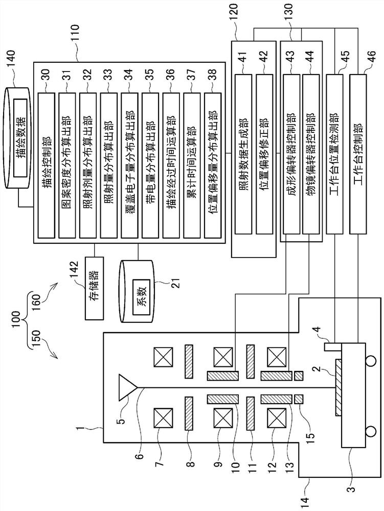
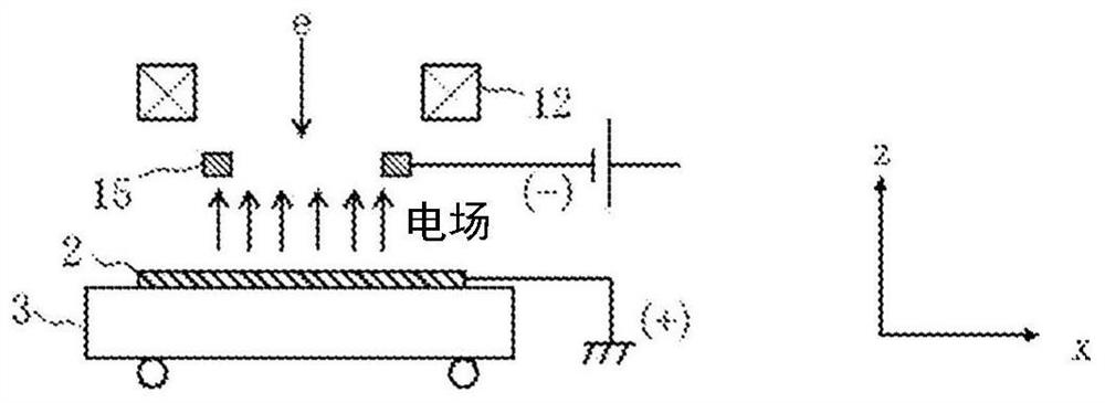
[0029] figure 1 It is a schematic configuration diagram of the rendering device according to the embodiment. figure 1 The illustrated rendering device 100 includes a rendering unit 150 and a control unit 160 . The drawing device 100 is an example of an electron beam drawing device. The drawing unit 150 has the electron column 1 and the drawing chamber 14 . An electron gun 5 , an illumination lens 7 , a first diaphragm 8 , a projection lens 9 , a forming deflector 10 , a second diaphragm 11 , an objective lens 12 , an objective lens deflector 13 , and an electrostatic lens 15 are disposed in the electron column 1 .

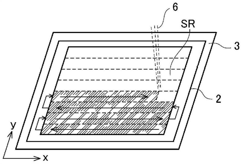
[0030] The XY stage 3 is arranged in the dra...


PUM


Abstract

The purpose of the present invention is to correct, in a highly accurate manner, positional displacement due to a charging phenomenon. A charged particle beam drawing device (100), provided with: an irradiation amount distribution calculation unit (33) for calculating the irradiation amount distribution of a charged particle beam using a pattern density distribution and dose distribution; a fogging charged particle amount distribution calculation unit (34) for convolution-integrating each of the irradiation amount distribution and the respective distribution function for a plurality of fogging charged particles, and thereby calculating a plurality of fogging charged particle amount distributions; a charge amount distribution calculation unit (35) for calculating the charge amount distribution due to direct charging using the pattern density distribution, the dose distribution, and the irradiation amount distribution, and calculating the charge amount distribution due to a plurality of fogging charges using the plurality of fogging charged particle amount distributions; a positional displacement amount calculation unit (38) for calculating the positional displacement amount of the drawing position on the basis of the charge amount distribution due to direct charging and the charge amount distribution due to the plurality of fogging charges; a correction unit (42) for correcting the irradiation position using the positional displacement amount; and a drawing unit (150) for irradiating the corrected irradiation position with a charged particle beam.

Description

technical field [0001] The present invention relates to a charged particle beam drawing device, a charged particle beam drawing method, and a program. Background technique [0002] Along with the high integration of LSI, the circuit line width required by semiconductor devices has become smaller and smaller year by year. In order to form a desired circuit pattern on a semiconductor device, a high-precision original drawing pattern (mask, or especially used in a stepper or scanning exposure device) that will be formed on quartz using a reduced projection exposure device is used. Also known as a reticle) reduction transfer method onto a wafer. High-precision original painting patterns are drawn by an electron beam drawing device, using so-called electron beam lithography. [0003] When an electron beam is irradiated to a substrate such as a mask, the irradiation position or its surroundings are charged by the electron beam irradiated in the past, and the irradiation position...

Claims


Application Information

Patent Timeline
Patent Type & Authority Applications(China)
IPC IPC(8): H01L21/027G03F7/20H01J37/305
CPCG03F7/20H01L21/0277H01J37/3174H01J37/3026H01J2237/31769H01J37/12H01L21/027G03F7/70008G03F7/70558H01J37/1472H01J37/153H01J2237/20228H01J2237/31761H01L21/0274
Inventor 野村春之中山田宪昭
Owner NUFLARE TECH INC
Why Eureka
Try Eureka