
Seed crystal pasting jig, flow guide assembly and method for pasting seed crystal on edge

A seed crystal and tooling technology, applied in the field of silicon carbide growth devices, can solve the problems of high difficulty in controlling the amount of pasting glue, easy formation of radial temperature gradients, and high difficulty in taking seed crystals, so as to reduce the risk of artificial crystal defects and reduce planning. damage, the effect of improving uniformity

Inactive Publication Date: 2021-05-28
HUNAN SANAN SEMICON CO LTD
View PDF5 Cites 4 Cited by
  • Summary
  • Abstract
  • Description
  • Claims
  • Application Information

AI Technical Summary

Problems solved by technology

This method has high requirements on the pasting process (including the processing accuracy of the seed crystal plate and the uniformity of glue coating). If the glue on the back of the graphite paper is unevenly pasted, it is very easy to form a radial temperature gradient, resulting in produce defects
At the same time, it is difficult to control the amount of glue pasted on the entire back, and it is easy to leave residual glue on the front of the seed crystal.
In addition, it is difficult to take the seed crystal by the traditional pasting method, and it is easy to cause damage to the crystal due to human error

Method used


Image

  • Seed crystal pasting jig, flow guide assembly and method for pasting seed crystal on edge
  • Seed crystal pasting jig, flow guide assembly and method for pasting seed crystal on edge
  • Seed crystal pasting jig, flow guide assembly and method for pasting seed crystal on edge

Examples


Embodiment 1

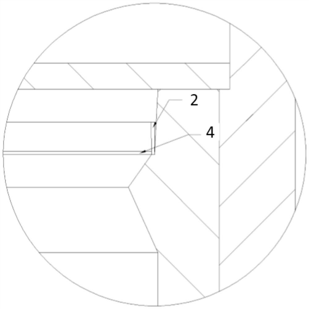
[0044] see figure 1 , the present embodiment provides a seed crystal pasting jig (ie pasting jig 3). A pasting outer ring 1 is provided on the outer periphery of the pasting jig 3 . The pasting jig 3 has a seed crystal bearing surface, and grooves are arranged on the seed crystal bearing surface for pasting graphite paper. Specifically, graphite paper 2 is arranged in the groove, and seed crystals 4 are arranged on the pasting jig 3 . Spatially, the graphite paper 2 ring is arranged around the seed crystal 4, and the shape of the seed crystal 4 is the original sheet.

[0045] The specifications of graphite paper 2 are as follows: the material is high-density graphite paper, the thickness is 0.5-1mm, the width is 15-20mm, and the length is 320-350mm. In this embodiment, the graphite paper 2 is set to have a thickness of 0.5 mm, a width of 15 mm, and a length of 320 mm.

[0046] The specifications of the sticking fixture 3 are as follows: it is made of high-density graphite,...

Embodiment 2

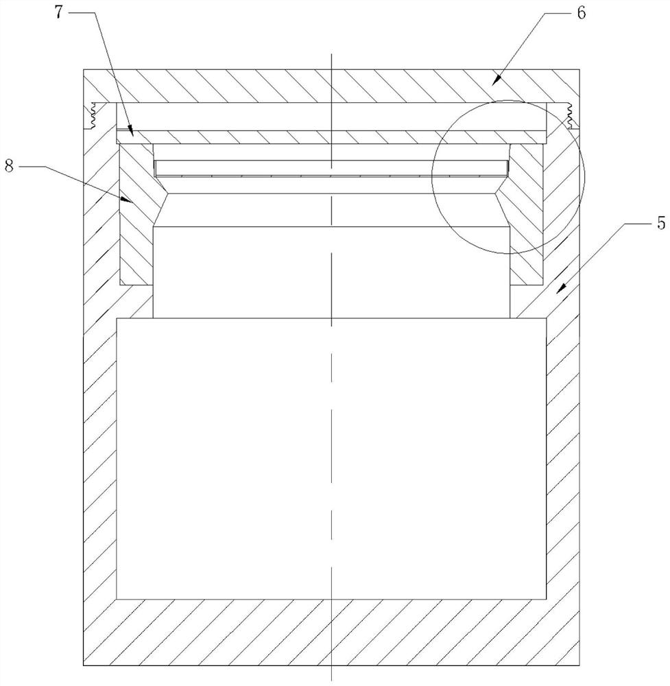
[0050] This embodiment provides a flow guide assembly and a crucible. Guide assembly and crucible reference figure 2 and image 3 shown.

[0051] The diversion assembly includes a seed paste jig, graphite paper 2 and a diversion cylinder 8 . Specifically, the pasting jig 3 for removing and pasting the outer ring 1 in Embodiment 1 is placed in the guide tube 8 . Bond the pasting tool 3 and the guide tube 8 with carbon glue, and then put them into a curing furnace for curing. Then put the cured guide tube 8 into the crucible, and use it to grow the crystal after assembling the thermal field.

[0052] The guide tube 8 in this embodiment is made of high-density graphite with a thickness of 2.95-3.05 mm. The first cavity, the second cavity and the third cavity are arranged in order from top to bottom, the first cavity is a conical cavity, the second cavity is a cavity formed by the combination of two conical structures, and The ends of the two circular platforms with smaller...

Embodiment 3

[0057] This embodiment provides a method for seed crystal growth, which includes: pasting the seed crystal 4 and the graphite paper 2 through the sticking jig 3 , and scraping off the graphite paper 2 put into the sticking jig 3 . Then put the treated seed crystal and graphite paper into the guide tube 8, use carbon glue to paste the graphite paper 2 and the inner wall of the guide tube 8, and put it into a curing furnace for curing. Select the crucible main body 5 with a thickness of 10mm, put 1.25kg of high-purity SIC powder into the barrel of the crucible main body 5, make it as smooth as possible, and then put the barrel of the crucible main body 5 into the cured guide tube 8. Cover the pressing plate 7 and the crucible lid 6. A cylindrical hard felt with a thickness of 1.5 mm is placed outside the crucible as a thermal insulation field.

[0058] The growth direction of the crystal is vertical to the horizontal plane where the seed crystal is located and grows downward. ...


PUM

PropertyMeasurementUnit
thicknessaaaaaaaaaa
diameteraaaaaaaaaa
widthaaaaaaaaaa

Abstract

The invention provides a seed crystal pasting jig, a flow guide assembly and a method for pasting a seed crystal on an edge, and relates to the technical field of silicon carbide growth devices. The seed crystal pasting jig is provided with a seed crystal bearing face, a groove is formed in the seed crystal bearing face to paste graphite paper, and a pasting outer ring is arranged in the direction, away from the circle center of the seed crystal bearing face, of the groove. According to the invention, an air layer can be established on the back of the seed crystal through the seed crystal pasting jig, so that the temperature uniformity of the back of the seed crystal can be effectively improved, thereby remarkably improving the quality of the crystal. Meanwhile, when the seed crystal pasting jig provided by the invention is used for crystal growth, the adhesive in the groove and the graphite paper attached with the adhesive are removed in advance, so that the residual adhesive on the surface of the seed crystal can be reduced to a great extent.

Description

technical field [0001] The invention relates to the technical field of silicon carbide growth devices, in particular to a seed crystal pasting jig, a diversion component and a method for pasting seed crystals on edges. Background technique [0002] With the advent of the era of big data, the popularization of 5G technology has become the general trend, and the demand for silicon carbide crystals as an efficient semiconductor material is also increasing. At the same time, the growth technology of silicon carbide is not very mature, and solving the technical bottleneck of silicon carbide single crystal growth has become one of the tasks of 5G promotion. At present, the main way of growing silicon carbide single crystal is through physical vapor deposition method (PVT method), through which 4 / 6 inch SiC single crystal can be grown. [0003] At present, the PTV method mainly grows crystals by pasting graphite paper on the back of the seed crystal. This method has high requirem...

Claims


Application Information

Patent Timeline
Patent Type & Authority Applications(China)
IPC IPC(8): C30B23/00C30B29/36
CPCC30B23/00C30B23/002C30B29/36
Inventor 李泉顺张洁付芬邓树军
Owner HUNAN SANAN SEMICON CO LTD
Learn More