Circuit Design and Modeling Method of a Balanced HTS Receiver
A high-temperature superconducting and circuit design technology, applied in CAD circuit design, computer-aided design, calculation, etc., can solve the problem of poor anti-noise performance of receivers, and achieve the effect of improving frequency conversion gain, fast attenuation, and small size
- Summary
- Abstract
- Description
- Claims
- Application Information
AI Technical Summary
Problems solved by technology
Method used
Image
Examples
Embodiment 1
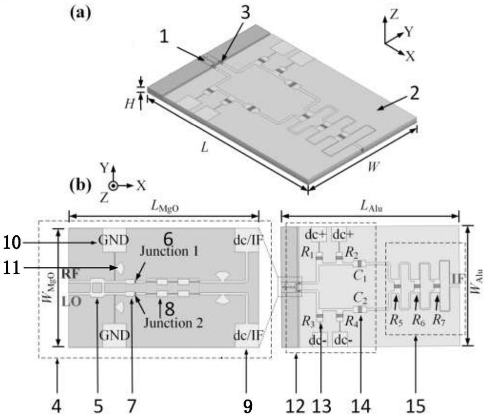
[0072] The circuit design of the balanced high-temperature superconducting receiver designed in this example, the design method corresponds to step 1 of the content of the invention, such as figure 1 As shown, it includes a MgO chip 1 and an alumina PCB 2 connected by an adhesive tape 3 .
[0073] Corresponding to step 1.1 of the content of the invention, design the MgO chip 1, the main design content is the high temperature superconducting microstrip circuit 4, first design the orthogonal coupling network 5 composed of 3dB branch bridges, as the orthogonal coupling circuit of the radio frequency signal and the local oscillator signal , to complete the quadrature coupling of the radio frequency signal and the local oscillator signal, and distribute the coupled signal energy equally to two signal outputs. Then design a quarter-wavelength high and low impedance line 7 for impedance matching, so that the coupled two-way radio frequency signals and local oscillator signals and loc...
Embodiment 2
[0080] The modeling method of the balanced high-temperature superconducting receiver of the present invention provides a powerful tool for the frequency mixing analysis and performance prediction of the balanced high-temperature superconducting receiver, and establishes a multi-port network interweaving model;
[0081] During specific implementation, the working process of the multi-port network interweaving model established in step 2.1 is as follows:
[0082] 1) The local oscillator current I is output by the local oscillator coupling network lo1 and I lo2 reach two Josephson junctions respectively;
[0083] 2) The RF current I at the output terminal of the RF signal coupling network rf1 and I rf2 reach two Josephson junctions respectively;
[0084] 3) Local oscillator current I lo1 and RF current I rf1 Nonlinear mixing at a Josephson junction; LO current I lo2 and RF current I rf2 nonlinear mixing at a Josephson junction;
[0085] 4) The intermediate frequency sign...
Embodiment 3
[0215] The performance prediction of the balanced high-temperature superconducting receiver described in the invention can effectively predict the DC IV characteristics, noise and conversion performance of the receiver.
[0216] For the balanced high-temperature superconducting receiver circuit designed in Example 1, carry out electromagnetic simulation design, and extract the self-impedance and mutual impedance of radio frequency signal, local oscillator signal, image signal and intermediate frequency coupling network from the electromagnetic simulation of this circuit design; Through two biased three-way circuits 12, the junction resistance R of the Josephson junction at different temperatures is measured j and critical current I j ; Finally, the above values are brought into the modeling method of the balanced high-temperature superconducting receiver derived in Example 2, and the DC IV characteristics, noise and conversion performance of the receiver are calculated by us...
PUM
 Abstract
Description
Claims
Application Information


