Small-pixel infrared focal plane detector based on metasurface lens

An infrared focal plane and detector technology, applied in electrical components, semiconductor devices, sustainable manufacturing/processing, etc., can solve problems such as effective fill factor decrease, optical coupling loss increase, pixel size reduction, etc., to achieve photoelectric crosstalk Effects of suppression, dark current reduction, and volume reduction

Inactive Publication Date: 2021-06-22
SHANGHAI INST OF TECHNICAL PHYSICS - CHINESE ACAD OF SCI
View PDF11 Cites 4 Cited by
  • Summary
  • Abstract
  • Description
  • Claims
  • Application Information

AI Technical Summary

Problems solved by technology

As the pixel size decreases, the effective fill factor decreases and optical coupling losses increase
At present, the commonly used traditional plano-convex microlenses rely on the phase difference caused by the thickness difference to achieve focusing. It is difficult to further reduce the image distance and pixel size under the premise of ensuring high optical coupling efficiency.

Method used


Image

  • Small-pixel infrared focal plane detector based on metasurface lens
  • Small-pixel infrared focal plane detector based on metasurface lens
  • Small-pixel infrared focal plane detector based on metasurface lens

Examples


Embodiment 1

[0027] See Figure 5 , the present embodiment provides an InP-based avalanche photodiode (APD) infrared focal plane detector based on a metasurface lens, including an InP-based avalanche photodiode focal plane and a metasurface lens (1) at a substrate;

[0028] InP-based APD infrared focal plane detector, including N-type InP substrate (1), APD epitaxial layer (4), P+ type doped region (5), N+ electrode (2) and P+ electrode (6) and SiNx passivation layer (7).

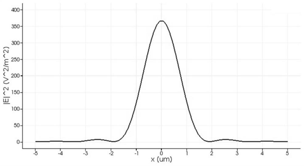
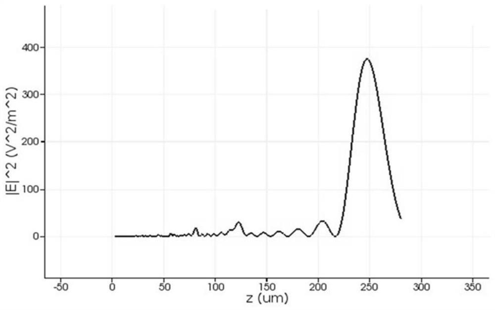
[0029] Wherein the InP-based APD infrared focal plane detector has a pixel diameter of about 3um, the metasurface lens (1) is etched on an InP substrate, and the focus of the metasurface lens is on the absorption layer of the APD pixel.

[0030] The working wavelength of the InP-based APD infrared focal plane detector of the metasurface lens is about 1550nm, and the metasurface lens is composed of a cylindrical array arranged according to the phase law, see figure 1 , the period of each cell is the distance between th...


PUM


Abstract

The invention discloses a small-pixel infrared focal plane detector based on a metasurface lens. The small-pixel infrared focal plane detector based on the metasurface lens comprises an infrared focal plane detector body and the metasurface lens formed at a substrate. The metasurface lens is composed of a plurality of small cylinders with sub-wavelength scales, the positions and the diameters of the small cylinders are arranged according to a phase rule, and the metasurface can modulate wavefront of incident light so that the incident light can be focused on an absorption layer of a detector pixel. Compared with a traditional infrared focal plane detector, the infrared focal plane detector has the advantages that focusing light spots in the sub-wavelength magnitude can be achieved, the pixel size can be reduced to the wavelength magnitude, and development of a planar focal plane device towards smaller pixels and higher pixel density is facilitated. Meanwhile, under the condition that the light response of the device is not changed or improved, the dark current of the device is reduced, the signal-to-noise ratio is improved, and photoelectric crosstalk between pixels is inhibited.

Description

technical field [0001] The invention relates to an infrared focal plane detector and a metasurface micro-nano structure with a focusing effect, in particular to an InP-based avalanche photodiode (APD) focal plane detector with a small pixel and high pixel density. Incident photodetector. Background technique [0002] With the development of the times, the status of photoelectric detectors is gradually improving. In aerospace, military industry, and civil automatic driving and communications, photoelectric detectors play an indispensable role, especially infrared focal plane detectors. It is developing towards the trend of large area array, small pixel and high density. [0003] Dark current, photoresponse, uniformity, crosstalk, etc. are several important indicators for evaluating focal plane detectors. As the area array becomes larger and larger, considering the uniformity and device size factors, the size of a single pixel is getting smaller and smaller. How to ensure hi...

Claims


Application Information

Patent Timeline
Patent Type & Authority Applications(China)
IPC IPC(8): H01L31/0232H01L31/101H01L31/18
CPCH01L31/02325H01L31/101H01L31/18Y02P70/50
Inventor 王文娟诸毅诚李冠海陆卫陈平平陈效双曲会丹高万甜
Owner SHANGHAI INST OF TECHNICAL PHYSICS - CHINESE ACAD OF SCI
Why Eureka
Try Eureka