A kind of gallium nitride-based green laser and preparation method thereof

A gallium nitride-based, laser technology, used in lasers, laser parts, semiconductor lasers, etc., can solve problems such as weak luminous intensity, reduce optical absorption loss, increase green light luminous intensity, and improve quantum efficiency.

Active Publication Date: 2022-08-02
DONGGUAN UNIV OF TECH
View PDF8 Cites 0 Cited by
  • Summary
  • Abstract
  • Description
  • Claims
  • Application Information

AI Technical Summary

Problems solved by technology

[0006] In order to overcome the defect of weak luminous intensity described in the above-mentioned prior art, the present invention provides a gallium nitride-based green laser, which has an InGaN / InGaN quantum well structure with variable temperature and variable growth rate as an effective Source region, and gradient doped u-InGaN+u-GaN+p-GaN+p + - AlGaN composite upper waveguide layer structure, which can effectively reduce the optical absorption loss of the P-type layer of the laser and improve the luminous intensity of green light

Method used


Image

  • A kind of gallium nitride-based green laser and preparation method thereof
  • A kind of gallium nitride-based green laser and preparation method thereof
  • A kind of gallium nitride-based green laser and preparation method thereof

Examples


Embodiment 1

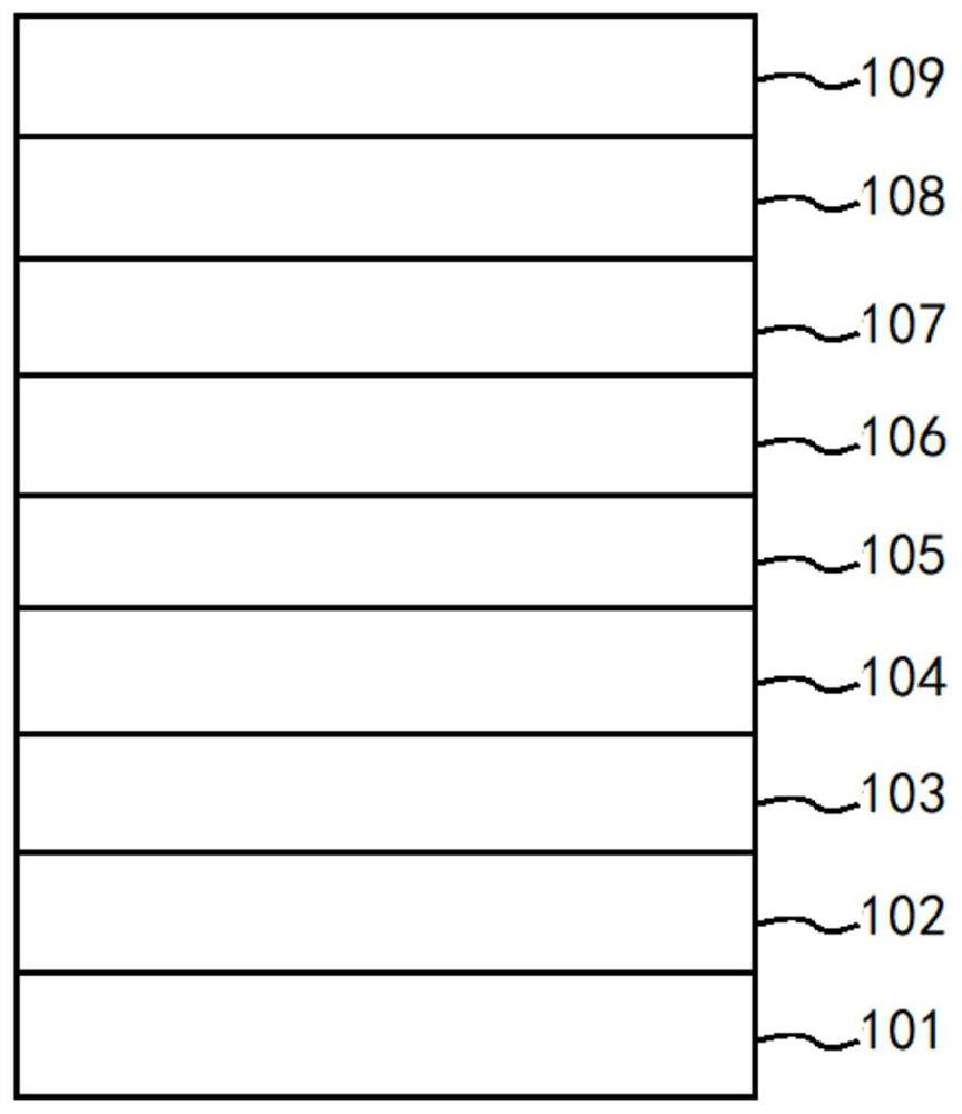
[0073] This embodiment provides a GaN-based green laser, such as figure 1 As shown, it includes a gallium nitride single crystal substrate 101, an n-GaN layer 102, an n-AlGaN / GaN superlattice confinement layer 103, a lower waveguide layer 104, an active region 105, a p Type electron blocking layer 106 , upper waveguide layer 107 , p-AlGaN / GaN superlattice confinement layer 108 , p-GaN contact layer 109 .

[0074] The GaN-based green laser is prepared through the following steps:

[0075] S1. First, in a metal-organic compound vapor phase epitaxy reaction chamber, in a hydrogen atmosphere, the temperature is raised to 500-700 °C, and then ammonia gas is introduced to form a mixed atmosphere of hydrogen and ammonia gas, and then the temperature is raised to 900-1100 °C. The single crystal substrate is subjected to surface activation treatment for 3 to 15 minutes.

[0076] S2. In a hydrogen atmosphere, at a temperature of 950-1200 °C, feed trimethyl gallium as the III group sou...

Embodiment 2

[0106] This embodiment provides a GaN-based green laser, such as figure 1 As shown, it includes a gallium nitride single crystal substrate 101, an n-GaN layer 102, an n-AlGaN / GaN superlattice confinement layer 103, a lower waveguide layer 104, an active region 105, a p Type electron blocking layer 106 , upper waveguide layer 107 , p-AlGaN / GaN superlattice confinement layer 108 , p-GaN contact layer 109 .

[0107] The GaN-based green laser is prepared through the following steps:

[0108] S1. First, in a metal-organic compound vapor phase epitaxy reaction chamber, in a hydrogen atmosphere, the temperature is raised to 500-700 °C, and then ammonia gas is introduced to form a mixed atmosphere of hydrogen and ammonia gas, and then the temperature is raised to 900-1100 °C. The single crystal substrate is subjected to surface activation treatment for 3 to 15 minutes.

[0109] S2. In a hydrogen atmosphere, at a temperature of 950-1200 °C, feed trimethyl gallium as the III group sou...


PUM

PropertyMeasurementUnit
thicknessaaaaaaaaaa
thicknessaaaaaaaaaa
thicknessaaaaaaaaaa

Abstract

The invention discloses a gallium nitride-based green laser and a preparation method thereof. A gallium nitride-based green laser, including a gallium nitride single crystal substrate, an n-GaN layer, an n-AlGaN / GaN superlattice confinement layer, a lower waveguide layer, an active region, a p type electron blocking layer, upper waveguide layer, p-AlGaN / GaN superlattice confinement layer, p-GaN contact layer; the active region is a quantum well structure with variable temperature and growth rate, and the lower waveguide layer and the upper waveguide layer are gradients Doped composite waveguide layer. In the present invention, the InGaN / InGaN quantum well structure with variable temperature and growth rate is set as the active region, and the gradient doped u-InGaN+u-GaN+p-GaN+p + ‑AlGaN composite upper waveguide layer, and gradient doped n + ‑Al y1 Ga 1‑y1 N+n‑GaN+u‑GaN+u‑In x5 Ga 1‑x5 The N composite lower waveguide layer effectively reduces the optical absorption loss of the P-type layer of the laser, improves the quantum efficiency of the laser, and further improves the green light emitting intensity of the GaN-based green laser.

Description

technical field [0001] The invention relates to the technical field of semiconductor optoelectronics, and more particularly, to a gallium nitride-based green laser and a preparation method thereof. Background technique [0002] Group III-V nitride semiconductor materials, including gallium nitride (GaN), aluminum nitride (AlN) and indium nitride (InN) and their alloys, group III-V nitrides are next to silicon and gallium arsenide. The third-generation semiconductor material is an ideal material for making semiconductor lasers from ultraviolet to green wavelengths. [0003] GaN-based green lasers have important application value in the fields of laser display, biomedicine, material processing, optical communication, optical storage, instrument and detection, and image recording. At present, the most eye-catching application field of GaN-based semiconductor lasers is laser display. Laser display is a display technology with red, green and blue lasers as the light source, whic...

Claims


Application Information

Patent Timeline
Patent Type & Authority Patents(China)
IPC IPC(8): H01S5/343H01S5/20
CPCH01S5/343H01S5/2018H01S5/2031
Inventor 贾传宇
Owner DONGGUAN UNIV OF TECH
Why Eureka
Try Eureka