Electrode and preparation method thereof
A technology of electrodes and conductive substances, which is applied in the field of electrodes and their preparation, can solve the problems of complex preparation methods for thick electrodes, uncontrollable pore structure and distribution of thick electrodes, and inconvenient expanded production, so as to facilitate expanded production and methods Simple and easy to implement, the effect of solving processing problems
- Summary
- Abstract
- Description
- Claims
- Application Information
AI Technical Summary
Problems solved by technology
Method used
Image
Examples
Embodiment 1
[0059] Production of the positive electrode sheet:
[0060] 1. Mix the positive electrode active material nickel cobalt lithium manganate (NCM), carbon nanotube conductive agent (CNTs), and binder polyvinylidene fluoride (PVDF) in a weight ratio of 96.5:0.5:3, and then add N-formazan Base pyrrolidone (NMP), make NMP account for 45% of the weight of the whole mixture, stir for 3-5h to obtain positive electrode slurry.
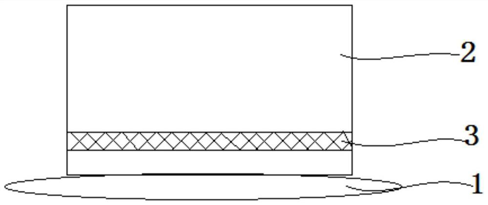
[0061] 2. Coating the slurry containing the active material and the conductive material on the aluminum current collector 1 , drying at 110° C. for tens of seconds to obtain the first active layer 2 with a thickness of 50 μm.
[0062] 3. Spinning a polyacrylonitrile fiber web on the active layer 2 using an electrospinning device. The ratio of polyacrylonitrile:N,N-dimethylformamide (DMF) in the spinning solution is 600mg:10ml, the spinning voltage is 15kV, the distance between the needle tip and the substrate is 15cm, the thickness of the fiber mat is controlle...
Embodiment 2
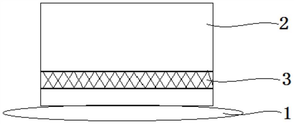
[0072] The manufacturing process of the positive and negative electrodes and the battery is basically the same as in Example 1, except that the thickness of the polyacrylonitrile fiber web in Example 1, that is, the thickness of the through-hole layer is changed to 10 μm.
Embodiment 3
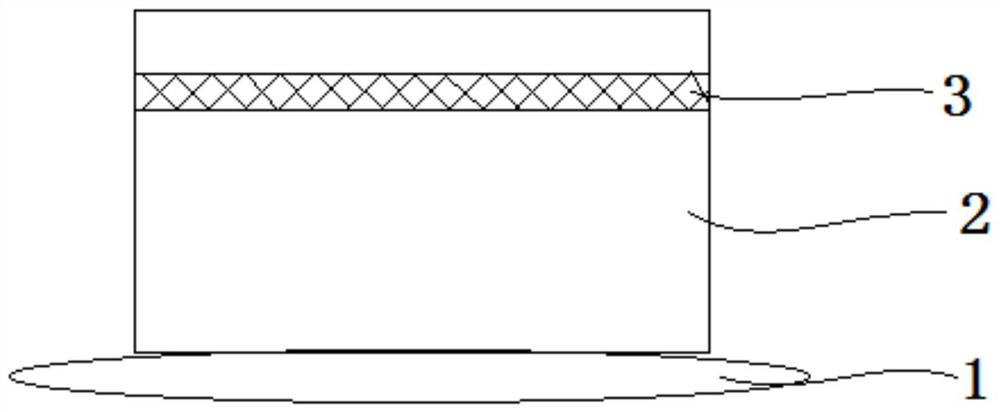
[0074] The manufacturing process of the positive and negative electrodes and the battery is basically the same as in Example 1, except that the thickness of the first active layer 2 in Example 1 is changed to 245 μm, and the thickness of the second active layer 2 is changed to 50 μm.
PUM
| Property | Measurement | Unit |
|---|---|---|
| Thickness | aaaaa | aaaaa |
| Thickness | aaaaa | aaaaa |
| Thickness | aaaaa | aaaaa |
Abstract
Description
Claims
Application Information


